
MicroLED display device based on quantum dot color conversion layer and preparation method of MicroLED display device

A technology for color conversion layers and display devices, applied in semiconductor devices, electrical solid devices, electrical components, etc., can solve the problems of waste of quantum dots, reduce conversion efficiency, and limit equipment accuracy, and achieve the effect of fewer steps and suppressing stray light.

Active Publication Date: 2021-04-09
CHANGCHUN INST OF OPTICS FINE MECHANICS & PHYSICS CHINESE ACAD OF SCI
View PDF17 Cites 1 Cited by
  • Summary
  • Abstract
  • Description
  • Claims
  • Application Information

AI Technical Summary

Problems solved by technology

Inkjet printing technology is limited by the accuracy of equipment. Inkjet printing is difficult to control uniformity and prone to "coffee ring effect", and it is difficult to realize when the pattern is less than 20μm; while photoresist doped patterning technology can achieve The preparation of small-sized pixels below 10 μm, but the doped photolithography machine is easy to degrade the quantum dots and reduce their conversion efficiency. In addition, this method causes a lot of waste of quantum dots

Method used


Image

  • MicroLED display device based on quantum dot color conversion layer and preparation method of MicroLED display device
  • MicroLED display device based on quantum dot color conversion layer and preparation method of MicroLED display device
  • MicroLED display device based on quantum dot color conversion layer and preparation method of MicroLED display device

Examples


Embodiment 1

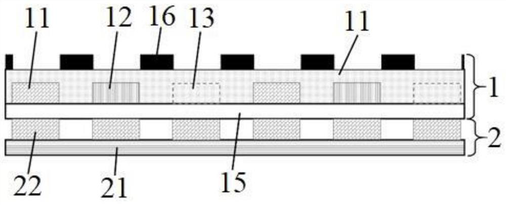
[0049] figure 1 The structure of the Micro LED display device based on the quantum dot color conversion layer according to Embodiment 1 of the present invention is shown.

[0050] Such as figure 1 As shown, the MicroLED display device based on the quantum dot color conversion layer includes a quantum dot color conversion layer 1 and a MicroLED array 2, and the MicroLED array 2 includes a driving substrate 21 and a plurality of LED chips 22, and a plurality of LED chips 22 are prepared on the driving substrate 21 , the driving substrate 21 is used to supply power to a plurality of LED chips 22 , and the plurality of LED chips 22 emit light under the power supply of the driving substrate 21 .

[0051] The quantum dot color conversion layer 1 is aligned and bonded to the MicroLED array 2, so that the light emitted by multiple LED chips 22 is converted into light of different colors through the quantum dot color conversion layer 1, thereby realizing a full-color MicroLED display ...

Embodiment 2

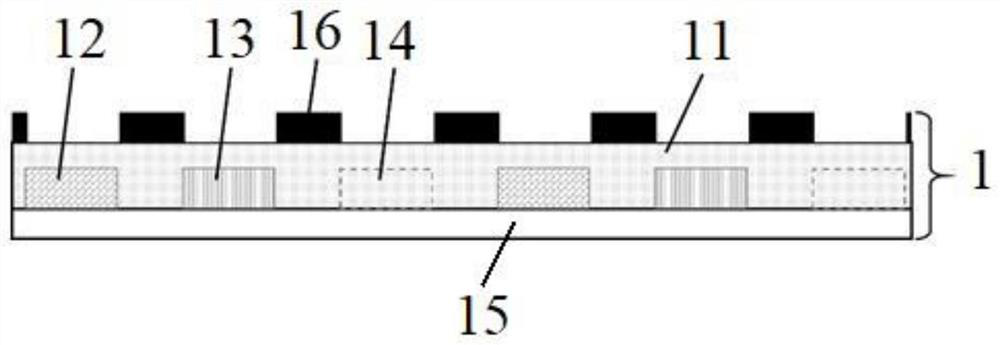
[0076] Figure 5 The structure of the Micro LED display device based on the quantum dot color conversion layer according to the second embodiment of the present invention is shown.

[0077] Such as Figure 5 As shown, the MicroLED display device 1 based on the quantum dot color conversion layer according to the second embodiment of the present invention includes a quantum dot color conversion layer 1 and a MicroLED array 2, and the MicroLED array 2 includes a driving substrate 21 and a plurality of LED chips 22, and the quantum dot The color conversion layer 1 is aligned and bonded to the MicroLED array 2, so that the light emitted by multiple LED chips 22 is converted into light of different colors through the quantum dot color conversion layer 1, thereby realizing a full-color MicroLED display device.

[0078] Image 6 It is the structure of the quantum dot color conversion layer according to the second embodiment of the present invention.

[0079] Such as Image 6 As sh...

Embodiment 3

[0083] Figure 7 The flow chart of the method for manufacturing the Micro LED display device based on the quantum dot color conversion layer according to the third embodiment of the present invention is shown.

[0084] Such as Figure 7 As shown, the preparation method of the Micro LED display device based on the quantum dot color conversion layer provided by the third embodiment of the present invention includes the following steps:

[0085] S1. Prepare the Micro LED display array and the quantum dot color conversion layer respectively, and align and bond the prepared Micro LED display array and the quantum dot color conversion layer to form a Micro LED display device.

[0086] Figure 8 The dynamic process of the preparation method of the quantum dot-based color conversion layer according to the third embodiment of the present invention is shown.

[0087] Such as Figure 7 and Figure 8 Commonly shown, the preparation method based on the quantum dot color conversion lay...


PUM


Abstract

The invention provides a MicroLED display device based on a quantum dot color conversion layer and a preparation method of the MicroLED display device. The MicroLED display device comprises a MicroLED array and the quantum dot color conversion layer bonded with the MicroLED array; the quantum dot color conversion layer comprises a micro-channel transparent substrate layer and a micro-channel revere mold layer which are bonded together; the micro-channel reverse mold layer comprises at least one pixel point; each pixel point comprises at least one group of quantum dot sites used for injecting a quantum dot solution, a liquid inlet hole used for realizing inflow of the quantum dot solution and a liquid outlet hole used for realizing outflow of the quantum dot solution; and the inlets and outlets of the quantum dot sites in the pixel points are respectively communicated with the corresponding liquid inlet holes and liquid outlet holes through micro-channels which are not crossed with one another; the quantum dot solution is injected into each group of quantum dot sites, and quantum dots for realizing color conversion are formed after photocuring is performed; and the quantum dots of the quantum dot color conversion layer are not doped with a photoresist, and the quantum dots are not degraded, so that the conversion efficiency of the quantum dots is not reduced, and a large amount of waste of the quantum dots is avoided.

Description

technical field [0001] The invention relates to the technical field of Micro LED display, in particular to a Micro LED display device based on a quantum dot color conversion layer and a preparation method thereof. Background technique [0002] Micro LED array usually refers to a two-dimensional array composed of high-density pixel light-emitting units integrated on a single chip. Usually the size of a single Micro LED is less than 100 μm. The integration of monochrome MicroLED array and color conversion layer is a relatively convenient and feasible method to realize full-color display of MicroLED. Different colors of quantum dot color conversion layers can be bonded to the single-color MicroLED array to convert the light emission of each MicroLED into different colors to form a full-color display of the MicroLED array. [0003] At present, the technologies for preparing quantum dot color conversion layers mainly include inkjet printing and photoresist doping and patterning...

Claims


Application Information

Patent Timeline
Patent Type & Authority Applications(China)
IPC IPC(8): H01L27/15H01L33/50
CPCH01L27/156H01L33/505H01L2933/0041
Inventor 陶金赵永周李阳梁静秋秦余欣吕金光王惟彪李盼园樊凯莉
Owner CHANGCHUN INST OF OPTICS FINE MECHANICS & PHYSICS CHINESE ACAD OF SCI
Learn More