SOI-based LDMOS device based on flexible substrate and manufacturing method thereof

A flexible substrate and device technology, applied in semiconductor/solid-state device manufacturing, semiconductor devices, electrical components, etc., can solve the problem of low mobility

Inactive Publication Date: 2021-04-09
XIDIAN UNIV +1
View PDF21 Cites 0 Cited by
  • Summary
  • Abstract
  • Description
  • Claims
  • Application Information

AI Technical Summary

Problems solved by technology

At present, there have been great breakthroughs in the development of flexible materials. For example, the mobility of organic materials based on rigid substrates has exceeded 100; however, the mobility of organic materials is still relatively low when based on flexible substrates with high surface roughness.

Method used


Image

  • SOI-based LDMOS device based on flexible substrate and manufacturing method thereof
  • SOI-based LDMOS device based on flexible substrate and manufacturing method thereof
  • SOI-based LDMOS device based on flexible substrate and manufacturing method thereof

Examples


Embodiment Construction

[0053] Below in conjunction with accompanying drawing, further describe the present invention in detail through embodiment.

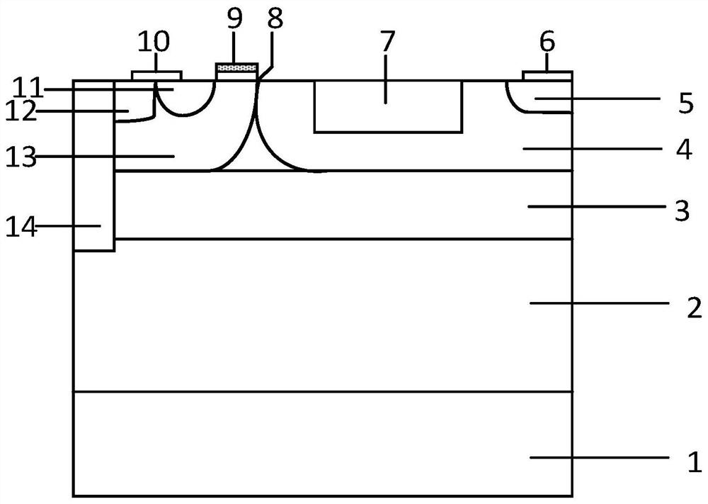
[0054] Such as figure 1 As shown, an SOI (Silicon-On-Insulator)-based lateral double-diffused metal-oxide-semiconductor field effect transistor (LDMOS) applied to a flexible electronic system has a structure of:

[0055] Substrate 1 of flexible material; PDMS, PET, PI, PEN and other flexible materials can be used, and the substrate thickness of the flexible material is 200-500 μm;

[0056] The P-type silicon layer 2 located on the surface of the substrate has a thickness of 2-10 μm;

[0057] The SOI base 3 located on the surface of the P-type silicon layer has a thickness of 1-3 μm;

[0058] The base region 13 and the drift region 4 formed by the epitaxial layer on the SOI base are relatively on the left and right sides respectively, with a thickness of 1-2 μm;

[0059] The source region formed on top of the base region is composed of P + District 1...


PUM

PropertyMeasurementUnit
thicknessaaaaaaaaaa
thicknessaaaaaaaaaa
thicknessaaaaaaaaaa

Abstract

The invention discloses an SOI-based LDMOS device based on a flexible substrate and a manufacturing method thereof, aims to further optimize the contradictory relation between breakdown voltage and specific on-resistance so as to optimize the performance of the device, and can be applied to a flexible electronic system. According to the device, a power device SOI LDMOS with excellent performance is combined with a flexible substrate, a P-type silicon substrate material with an SOI base is adopted, and a drift region and a base region are formed on an epitaxial layer on the SOI base through doping; a surface electrode is etched and deposited at the left end of the base region, wherein the surface electrode sequentially penetrates through the base region and the SOI base from the surface of the device along the longitudinal direction and goes deep into the upper part of the P-type silicon layer; and an oxidation groove filled with a dielectric material is formed in the surface of the middle region of the drift region. According to the invention, the power device SOI LDMOS is combined with the flexible substrate, so that new breakthrough and innovation in the fields of traditional inorganic semiconductor power devices and flexible electronics are realized, and the defect of poor electronic performance of flexible organic materials can be overcome.

Description

technical field [0001] The invention relates to the field of flexible electronic systems, in particular to an SOI (Silicon-On-Insulator)-based lateral double-diffused metal oxide semiconductor field effect transistor based on a flexible substrate and a manufacturing method thereof. Background technique [0002] One of the traditional inorganic semiconductor devices that can be used as switching power devices in integrated circuits is the SOI (Silicon-On-Insulator)-based lateral double-diffused metal-oxide-semiconductor field-effect transistor (Lateral Double-diffused MOSFET, referred to as LDMOS). Power devices have the advantages of fast speed, high integration, and low power consumption, and can be used in high-frequency and high-voltage integrated circuits. [0003] With the rapid development of the traditional inorganic semiconductor industry, its materials, devices and processes have also developed rapidly. Among them, the development of the electronic properties of in...

Claims


Application Information

Patent Timeline
Patent Type & Authority Applications(China)
IPC IPC(8): H01L29/78H01L21/336H01L29/06
CPCH01L29/0603H01L29/0615H01L29/0684H01L29/66681H01L29/7816H01L29/7824
Inventor 段宝兴唐春萍杨银堂
Owner XIDIAN UNIV
Why Eureka
Try Eureka