Embedded panel structure and manufacturing method thereof

A manufacturing method and embedded technology, applied in semiconductor/solid-state device manufacturing, data processing input/output process, instruments, etc., can solve problems such as excessive noise, high technical requirements, lower yield, etc., to reduce panel The effect of thickness, reducing pixel area and increasing aperture ratio

Pending Publication Date: 2021-04-13
FUJIAN HUAJIACAI CO LTD
View PDF0 Cites 0 Cited by
  • Summary
  • Abstract
  • Description
  • Claims
  • Application Information

AI Technical Summary

Problems solved by technology

However, when embedding the touch sensor into the pixel, the matching touch integrated circuit must also be embedded in it, otherwise it is easy to cause wrong touch sensing signals or excessive noise, and the complexity and difficulty of the manufacturing process are huge.
The organic layers in OLED are all attached by evaporation method, which requires high technical requirements and great difficulty, so the yield rate is also low. Adding a layer of touch IC in the evaporation structure will further reduce the yield rate. Therefore, the current OLED panel Embedded touch has yet to break through

Method used


Image

  • Embedded panel structure and manufacturing method thereof
  • Embedded panel structure and manufacturing method thereof
  • Embedded panel structure and manufacturing method thereof

Examples


Embodiment Construction

[0069] In order to explain in detail the technical content, structural features, achieved goals and effects of the technical solution, the following will be described in detail in conjunction with specific embodiments and accompanying drawings.

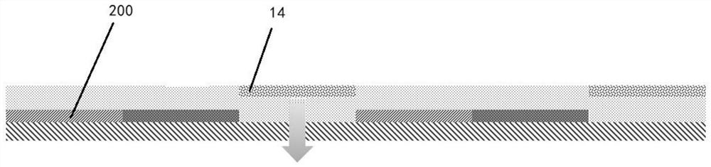
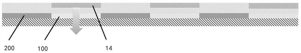
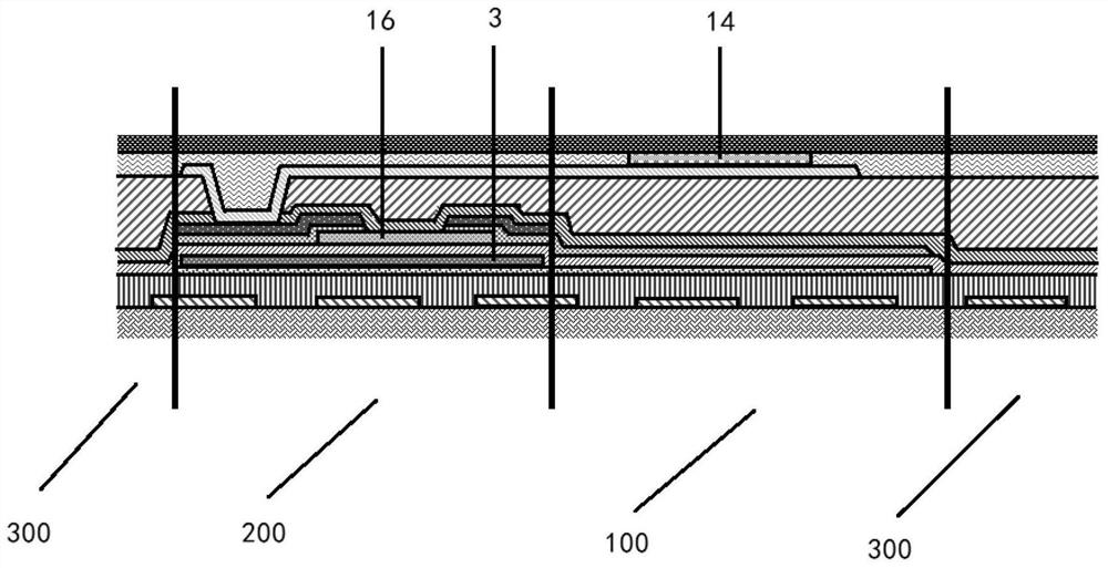
[0070] see Figure 1 to Figure 19 In this application, a method for manufacturing an embedded panel structure is provided, including the steps of: dividing the substrate 1 into a light-transmitting capacitor area 100, a TFT area 200, and a substrate area 300; please refer to Figure 17 to Figure 19 ,exist Figure 17 to Figure 19 The etching method of the gate metal layer 3 and the first light-transmitting conductive layer is listed in ; meanwhile, the manufacturing method of the second light-transmitting conductive layer and the source-drain metal layer is also the same, only the first light-transmitting conductive layer needs to be Layer is replaced by the second light-transmitting conductive layer, and the gate metal layer is repla...


PUM


Abstract

The invention discloses an embedded panel structure and a manufacturing method thereof. The manufacturing method comprises the following steps of manufacturing a first light-transmitting conductive layer and a gate metal layer, and manufacturing a first insulating layer, removing the first insulating layer on the substrate area, and removing the upper part of the first insulating layer on the light-transmitting capacitor area, removing the first light-transmitting conductive layer and the gate metal layer, ashing the first insulating layer, etching the gate metal layer, and removing the first insulating layer, manufacturing a second insulating layer, manufacturing an active layer, manufacturing a second light-transmitting conductive layer and a source-drain metal layer, and manufacturing a third insulating layer, removing the substrate area and the third insulating layer above the middle part of the active layer, removing the upper part of the third insulating layer on the light-transmitting capacitor area, removing the second light-transmitting conductive layer and the source-drain metal layer, removing the third insulating layer, etching the source-drain metal layer;, and removing the third insulating layer. By additionally arranging the light-transmitting capacitor area, the light-emitting layer can be not provided with a blank avoidance region, and light is directly emitted from the light-transmitting capacitor area, so that the area of a single pixel can be reduced, and the aperture opening ratio of a display area is improved.

Description

technical field [0001] The invention relates to the field of touch display screens, in particular to an embedded panel structure and a manufacturing method thereof. Background technique [0002] With the development of display technology, various new technologies are emerging. Transparent display technology has attracted more and more attention because of its transparent display panel and its unique application. Thin and transparent display is the future display. development trend. [0003] At present, the touch technology used in AMOLED panels is mainly divided into three types: Out-Cell, In-Cell and On-Cell. Out-cell technology is dominated by touch manufacturers. This technology can be divided into glass and film methods. The touch sensor is placed between the cover glass and the display module. The disadvantage is that it is thicker. It is not in line with the development direction of thinner and lighter displays. [0004] In-Cell embeds the touch module in the AMOLED...

Claims


Application Information

Patent Timeline
IPC IPC(8): H01L27/32H01L21/77G06F3/044G06F3/041
CPCG06F3/0412G06F3/044G06F2203/04103H10K59/40H10K59/1216H10K59/1201
Inventor 陈宇怀黄志杰
Owner FUJIAN HUAJIACAI CO LTD
Why Eureka
Try Eureka