Check patentability & draft patents in minutes with Patsnap Eureka AI!

AZO material nano resistive film and preparation method thereof

A resistive film and nanotechnology, applied in metal material coating process, gaseous chemical plating, coating and other directions, can solve the problems of environmental pollution, narrow Zn content range of AZO materials, and high price of film preparation.

Pending Publication Date: 2021-04-16
INST OF HIGH ENERGY PHYSICS CHINESE ACADEMY OF SCI
View PDF5 Cites 0 Cited by
  • Summary
  • Abstract
  • Description
  • Claims
  • Application Information

AI Technical Summary

Problems solved by technology

[0005] The mature resistive film is only W-Al 2 o 3 and Mo-Al 2 o 3 Both, but ALD precursor WF for growth of W or Mo 6 or MoF 6 It will cause serious pollution to the environment and is highly corrosive. The pipeline must be highly corrosion-resistant, so the requirements for atomic layer deposition equipment are very high, and the preparation price of the film is therefore high.
[0006] Resistivity at 10 4 ~10 10 When Ω*cm, the Zn content range (70%-73%) of AZO material is very narrow and difficult to control

Method used


Image

  • AZO material nano resistive film and preparation method thereof
  • AZO material nano resistive film and preparation method thereof
  • AZO material nano resistive film and preparation method thereof

Examples


Embodiment Construction

[0031] The following will be combined with Figure 5 The present invention is described in detail with specific examples.

[0032] According to one embodiment of the present invention, a kind of preparation method of the AZO material nano-resistance film applied on the microchannel plate comprises the following steps:

[0033] 1) Put the device substrate into the reaction chamber for evacuation, and heat the reaction chamber and maintain the temperature;

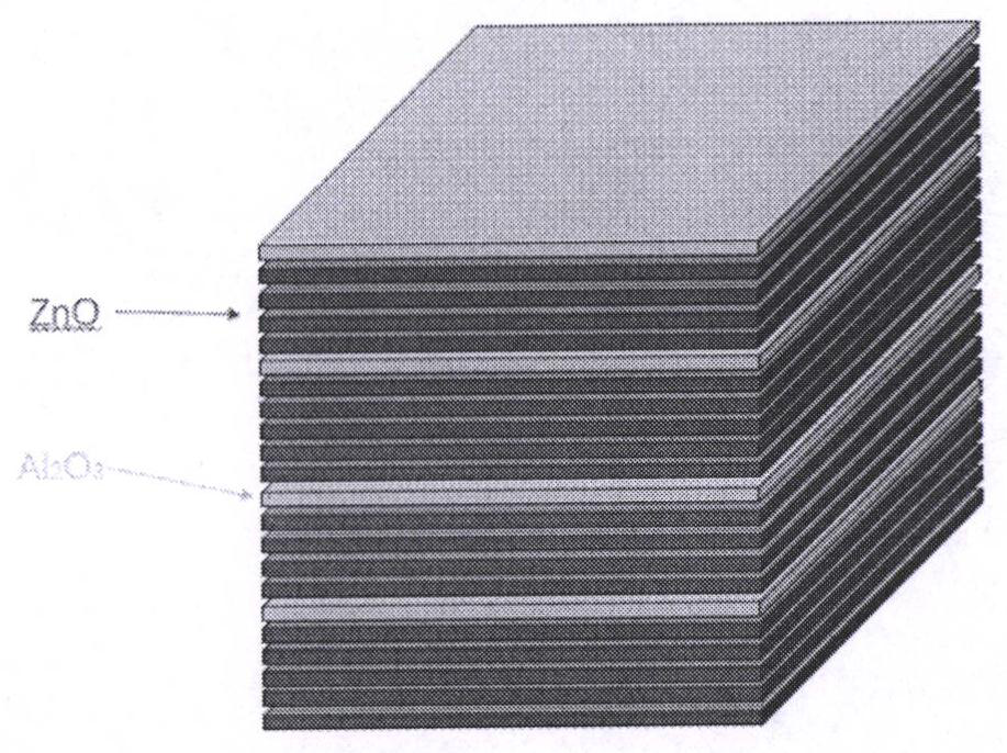
[0034] 2) Set Al 2 o 3 and ZnO atomic layer deposition process;

[0035] 3) Set the Al of the doping process by nesting small loops in large loops 2 o 3 and the atomic layer arrangement sequence of ZnO, so that the total number of atomic layer growth processes satisfies the range of 100 to 1000 for growth.

[0036] 4) Set the temperature of the reaction chamber to anneal the film.

[0037] 5) Growth Al 2 o 3 as the emission layer.

[0038] Further, the device substrate described in step 1) is an insulating micropor...


PUM


Abstract

The invention discloses an AZO material nano resistive film and a preparation method thereof, and belongs to the field of device materials. The 104-1010 ohm*cm nano resistive film is widely applied to the fields of micro-channel plates, single-channel electron multiplication, drift tubes, charge dissipation and discharge and the like, but the Zn content interval (70%-73%) of the AZO material in the resistivity interval is very narrow and is difficult to regulate and control. The method comprises the following steps: 1) putting a device substrate into a reaction chamber for vacuumizing, heating the reaction chamber and keeping the temperature; 2) setting an atomic layer deposition process of Al2O3 and ZnO; 3) setting the atomic layer arrangement sequence of Al2O3 and ZnO of the doping process in a large-cycle nested small-cycle mode for growth; and 4) setting the temperature of the reaction chamber to anneal the film. In the process, the AZO material can be used for regulating, controlling and optimizing the film within the interval of 101-1010 ohm*cm.

Description

technical field [0001] The invention belongs to the field of device materials and relates to an AZO material high-resistance thin film. Background technique [0002] Atomic layer deposition technology is a controllable rate of precursor gas and reaction gas alternately entering the substrate, physical and chemical adsorption or surface saturation reaction occurs on the surface, and the material is deposited layer by layer in the form of a single atomic film on the surface of the substrate. Technology. Based on self-limiting reactions, ALD can produce continuous pinhole-free films with excellent step coverage and control over atomic-scale film thickness and composition. al 2 o 3 The atomic layer deposition technology of ZnO and ZnO is very mature, and the precursor source materials TMA and DEZ are relatively cheap compared to other precursor sources. [0003] Resistivity at 10 4 ~10 10 The Ω*cm nano-resistive film is widely used in many fields, such as the field of micr...

Claims


Application Information

Patent Timeline
IPC IPC(8): C23C16/40C23C16/455C23C16/56
Inventor 王玉漫刘术林闫保军张斌婷谷建雨姚文静
Owner INST OF HIGH ENERGY PHYSICS CHINESE ACADEMY OF SCI
Features
  • R&D
  • Intellectual Property
  • Life Sciences
  • Materials
  • Tech Scout
  • Unparalleled Data Quality
  • Higher Quality Content
  • 60% Fewer Hallucinations
Learn More