Micro LED structure and color display device
A technology of LED structure and color display, applied in the direction of identification devices, instruments, electrical components, etc., to achieve high production efficiency and yield, improve photon utilization, and improve conversion efficiency.
- Summary
- Abstract
- Description
- Claims
- Application Information
AI Technical Summary
Problems solved by technology
Method used
Image
Examples
no. 1 example
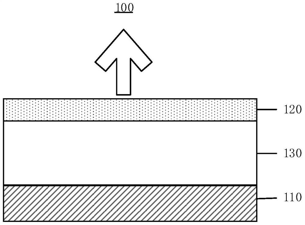
[0055] Please refer to figure 1 , the arrow in the figure indicates the direction of light emission. This embodiment provides a micro LED structure 100. The micro LED structure 100 includes a light emitting layer 130, a reflective layer 110 and a color selection layer 120, wherein the light emitting layer 130 is used for electroluminescence, reflective Layer 110 is on one side of light emitting layer 130 and color selection layer 120 is on the other side of light emitting layer 130 .
[0056] Specifically, the light-emitting layer 130 contains at least an electro-excitation material, and may also contain an electro-excitation material and multiple photo-excitation materials to achieve multi-wavelength excitation, wherein the electro-excitation material may be a quantum well, and the photo-excitation material may be a quantum dot.
[0057]The color selection layer 120 is used to select one color of light to pass through. The color selection layer 120 is a light wave filter inc...
no. 2 example
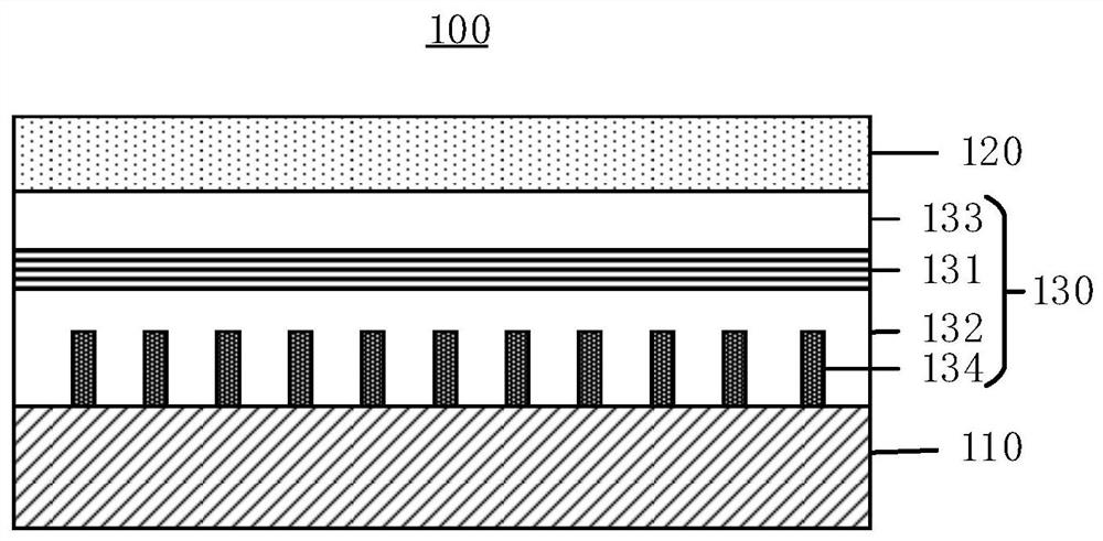
[0063] Please refer to figure 2 , this embodiment provides a micro-LED structure 100, the micro-LED structure 100 includes a light-emitting layer 130, a reflective layer 110 and a color selection layer 120, wherein the light-emitting layer 130 is used for electroluminescence, and the reflective layer 110 is located at the top of the light-emitting layer 130 On one side, the color selection layer 120 is located on the other side of the light emitting layer 130 .
[0064] Specifically, the light emitting layer 130 includes a quantum well layer 131 , a P-type semiconductor layer 132 , an N-type semiconductor layer 133 and a wavelength conversion material 134 .
[0065] The P-type semiconductor layer 132 is located on one side of the quantum well layer 131 , the N-type semiconductor layer 133 is located on the other side of the quantum well layer 131 , and the N-type semiconductor layer 133 is farther away from the reflective layer 110 than the P-type semiconductor layer 132 . T...
no. 3 example
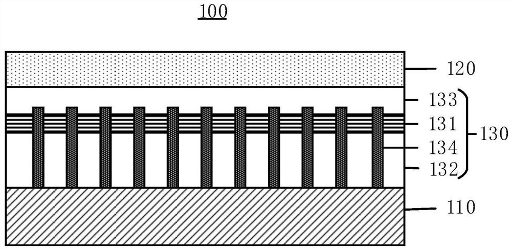
[0070] Please refer to image 3 , this embodiment provides a micro-LED structure 100, the micro-LED structure 100 includes a light-emitting layer 130, a reflective layer 110 and a color selection layer 120, wherein the light-emitting layer 130 is used for electroluminescence, and the reflective layer 110 is located at the top of the light-emitting layer 130 On one side, the color selection layer 120 is located on the other side of the light emitting layer 130 .
[0071] Specifically, the light emitting layer 130 includes a quantum well layer 131 , a P-type semiconductor layer 132 , an N-type semiconductor layer 133 and a wavelength conversion material 134 .
[0072] The P-type semiconductor layer 132 is located on one side of the quantum well layer 131 , and the N-type semiconductor layer 133 is located on the other side of the quantum well layer 131 . The quantum well layer 131 is used for electroluminescence, and the quantum well layer 131 can excite at least one short wave...
PUM
 Abstract
Description
Claims
Application Information


