Preparation method of nano array solar battery
A nano-array and solar cell technology, applied in the field of solar modules, can solve the problems of reducing photoelectric conversion efficiency, reducing the life of photo-generated carriers, and accelerating the recombination of photo-generated carriers, so as to improve photoelectric conversion efficiency, increase electron collection ability, Effect of improving photon utilization efficiency
- Summary
- Abstract
- Description
- Claims
- Application Information
AI Technical Summary
Problems solved by technology
Method used
Image
Examples
Embodiment 1
[0031] The preparation method of the nano-array solar cell of the present embodiment comprises the following steps:
[0032] (1) De-damaging and texturing of the silicon wafer surface: place the silicon wafer in an aqueous solution of nitric acid, hydrofluoric acid, and texturing additives, and the texturing time is 0.8 minutes; The volume ratio of 40%, 11%, 0.3% is mixed, and the concentrations of nitric acid, hydrofluoric acid and texturing additives are the same.
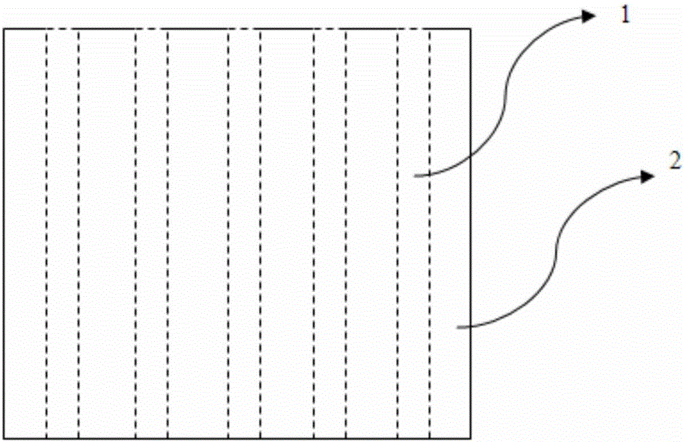
[0033] (2) Preparation of silicon wafer surface corrosion mask: use printing method to print negative polarity photoresist on the textured silicon wafer to prepare a surface corrosion mask, and the area 1 of the surface corrosion mask is as follows figure 1 As shown in , the thickness of the surface etching mask is 0.3 μm, and the width of the surface etching mask is 1.3 mm;
[0034] (3) Metal ion wet chemical catalytic corrosion nano-array preparation: the nano-array was prepared by hydrofluoric acid and silver...
Embodiment 2
[0043] The preparation method of the nano-array solar cell of the present embodiment comprises the following steps:
[0044] (1) De-damaging and texturing of the silicon wafer surface: place the silicon wafer in an aqueous solution of nitric acid, hydrofluoric acid, and texturing additives, and the texturing time is 0.8 minutes; The volume ratio of 40%, 11%, 0.3% is mixed, and the concentrations of nitric acid, hydrofluoric acid and texturing additives are the same.
[0045] (2) Preparation of silicon wafer surface corrosion mask: use printing method to print negative polarity photoresist on the textured silicon wafer to prepare a surface corrosion mask, and the area 1 of the surface corrosion mask is as follows figure 1 As shown in , the thickness of the surface etching mask is 0.3 μm, and the width of the surface etching mask is 1.3 mm;
[0046] (3) Metal ion wet chemical catalytic corrosion nano-array preparation: the nano-array was prepared by hydrofluoric acid and silver...
PUM
| Property | Measurement | Unit |
|---|---|---|
| Thickness | aaaaa | aaaaa |
| Width | aaaaa | aaaaa |
| Thickness | aaaaa | aaaaa |
Abstract
Description
Claims
Application Information
