Through hole forming method

A photoresist and preset position technology, which is applied in the direction of electrical components, semiconductor/solid-state device manufacturing, circuits, etc., can solve the problems of affecting the metal filling effect, difficult to control the etching morphology, and insufficient etching amount, etc., to achieve increased The effect of output yield, improvement of semiconductor device performance, and improvement of morphology

Inactive Publication Date: 2021-04-23
GREE ELECTRIC APPLIANCES INC
View PDF5 Cites 0 Cited by
  • Summary
  • Abstract
  • Description
  • Claims
  • Application Information

AI Technical Summary

Problems solved by technology

When etching contact holes in the wafer front process, it is difficult to control the etching morphology due to the small line width
Often the through hole is not opened due to insufficient etching amount, or the opening is too large due to over etching, which will affect the effect of metal filling

Method used


Image

  • Through hole forming method
  • Through hole forming method
  • Through hole forming method

Examples


Embodiment 1

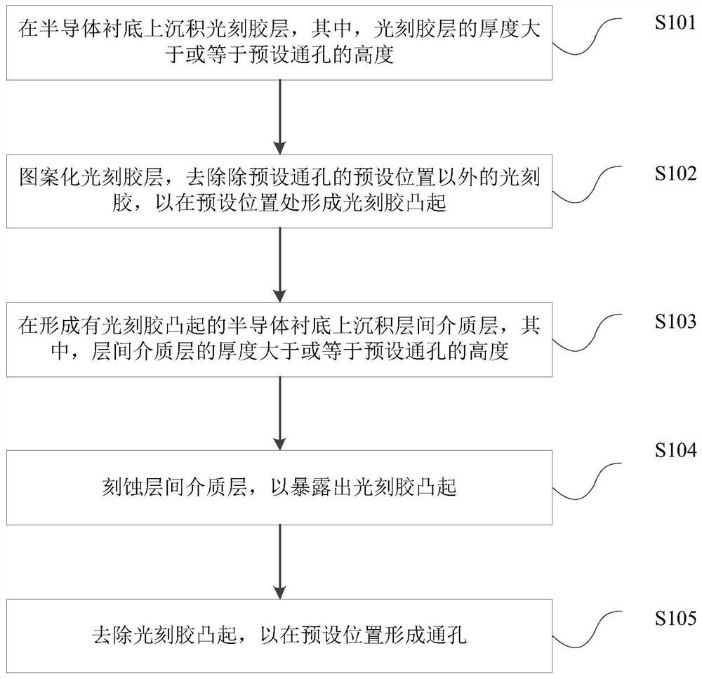
[0048] see figure 1 as shown, figure 1 It is a schematic flowchart of a method for forming a through hole provided in the embodiment of the present application, including step S101 to step S105.

[0049] In step S101 , a photoresist layer is deposited on the semiconductor substrate, wherein the thickness of the photoresist layer is greater than or equal to the height of the predetermined via hole.

[0050] This step can be to deposit a photoresist layer with a uniform thickness on the semiconductor substrate by spin coating. After the photoresist layer is formed, the photoresist layer can also be pre-baked to improve the photoresist layer in the subsequent exposure process. The exposure accuracy of the adhesive layer.

[0051] Wherein, since the photoresist layer needs to be able to form a photoresist protrusion at the preset position of the preset through hole in advance, the deposition thickness of the photoresist layer needs to be greater than or equal to the height of th...

Embodiment 2

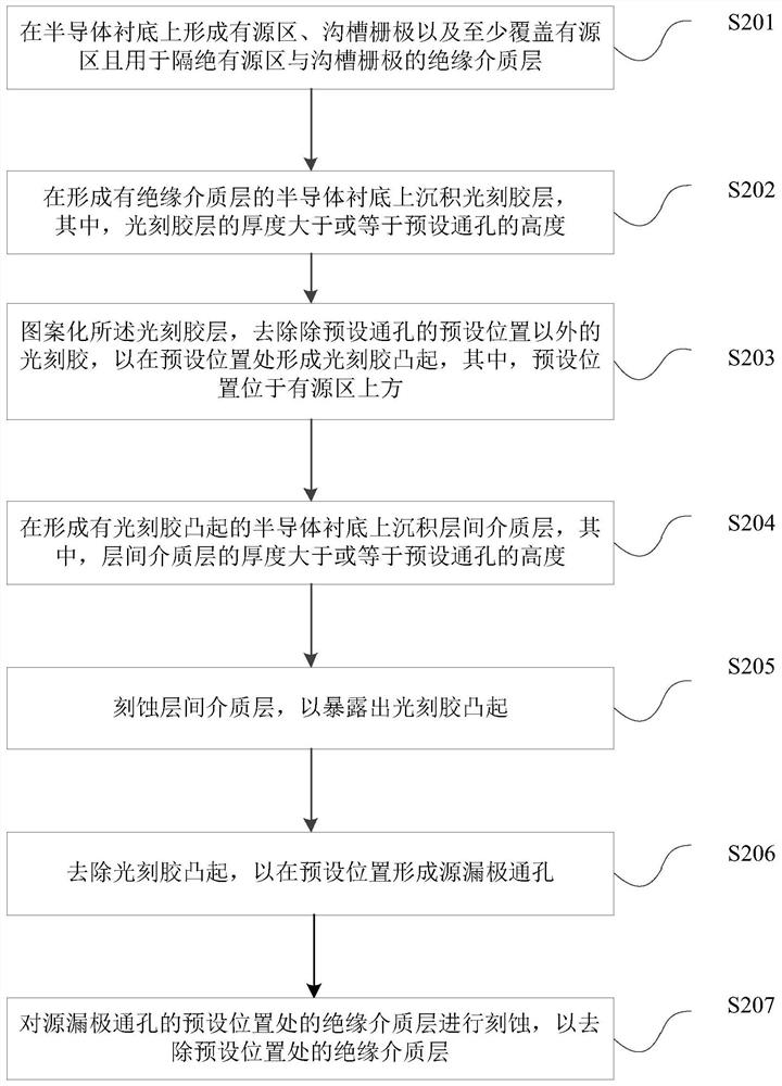
[0065] figure 2 It shows a schematic flowchart of the method for manufacturing semiconductor source-drain through holes provided by Embodiment 2 of the present application, including steps S201 to S207.

[0066] In step S201 , an active region, a trench gate, and an insulating dielectric layer covering at least the active region and used to isolate the active region and the trench gate are formed on a semiconductor substrate.

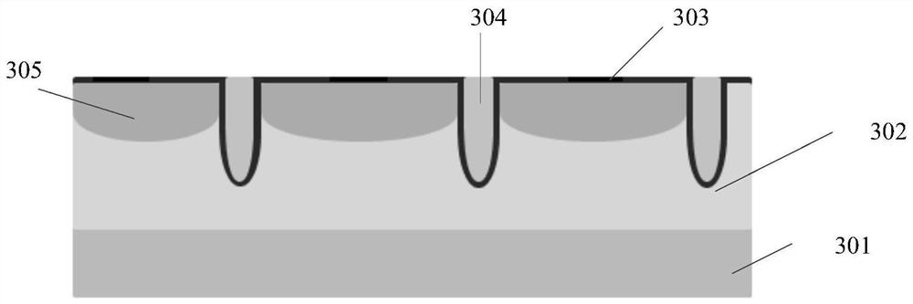
[0067] As an example, referring to FIG. 3(1), this step may specifically include providing a semiconductor substrate 301, growing an epitaxial layer 302 on the semiconductor substrate 301, and forming an epitaxial layer 302 by dry etching or wet etching. The groove of gate is formed on the layer 302, adopts chemical vapor deposition or the method of oxidizing the substrate to form a layer of insulating dielectric layer 303 covering the sidewall of the gate trench and the surface of the substrate, and the insulating dielectric layer 303 covered with Ma...

Embodiment 3

[0088] see Figure 4 , Figure 4A schematic flowchart of a method for manufacturing a semiconductor gate through hole provided by an embodiment of the present application is shown, including steps S401 to S406.

[0089] In step S401 , an active region, a trench gate, and an insulating dielectric layer covering at least the active region and used to isolate the active region and the trench gate are formed on a semiconductor substrate.

[0090] In step S402, a photoresist layer is deposited on the semiconductor substrate on which the insulating medium layer is formed, wherein the thickness of the photoresist layer is greater than or equal to the height of the predetermined via hole.

[0091] In this embodiment of the present application, steps S401 to S402 may be the same as steps S201 to S202 in Embodiment 2, and for the sake of brevity, details are not repeated here.

[0092] In step S403, the photoresist layer is patterned, and the photoresist is removed except the preset p...


PUM


Abstract

The invention discloses a through hole forming method. The method comprises the following steps of: depositing a photoresist layer on a semiconductor substrate, removing photoresist except a preset position of a preset through hole by patterning the photoresist layer, forming a photoresist bulge at the preset position of the through hole, and depositing an interlayer dielectric layer to cover the semiconductor substrate on which the photoresist bulge is formed; and etching the deposited interlayer dielectric layer until exposing the photoresist bulge; and finally, removing the photoresist to form the through hole at the preset position. The position of the through hole which is directly formed in the interlayer dielectric layer by etching in the prior art is covered by the photoresist in advance, so that a certain aperture ratio is ensured, the shape of the through hole is improved, subsequent metal filling is facilitated, electric leakage can be reduced, the output yield of a semiconductor device is increased, and the performance of the semiconductor device is improved.

Description

technical field [0001] The invention relates to the field of semiconductors, in particular to a method for forming a through hole. Background technique [0002] The ultra-thinning of semiconductor chips is a trend of technological progress, but at the same time it is also facing the problem of technological improvement. Among them, wafer contact hole etching is an essential process in the semiconductor chip manufacturing process. When etching contact holes in the wafer front process, it is difficult to control the etching morphology due to the small line width. Often, the through hole is not opened due to insufficient etching amount, or the opening is too large due to over-etching, which will affect the effect of metal filling. Contents of the invention [0003] The technical problem to be solved by the present invention is: it is difficult to control the etching morphology of the through hole in the prior art, which affects the performance of the semiconductor device. ...

Claims


Application Information

Patent Timeline
Patent Type & Authority Applications(China)
IPC IPC(8): H01L21/768H01L21/311
CPCH01L21/76802H01L21/311
Inventor 吴佳蒙史波肖婷敖利波
Owner GREE ELECTRIC APPLIANCES INC
Why Eureka
Try Eureka