Tunable fixedly-attached bulk acoustic wave resonator
A bulk acoustic wave resonator and paste-type technology, which is applied in the field of microelectronics, can solve the problems of affecting the performance of transceivers, the inability to integrate chips, and low Q value, and achieve the effects of simple structure, good mechanical stability, and easy production
- Summary
- Abstract
- Description
- Claims
- Application Information
AI Technical Summary
Problems solved by technology
Method used
Image
Examples
Embodiment 1
[0033] like Figure 1-2 As shown, the first tunable fixed-mount BAW resonator 11 provided in Embodiment 1 includes a substrate 12 , a piezoelectric oscillation stack 13 , an acoustic reflection structure 16 and a tuning structure 15 . There is a cavity 14 in the middle of the substrate 12; the tuning structure 15 sequentially includes a first electrode 15a, a piezoelectric layer 15b and a second electrode 15c from top to bottom; the acoustic reflection layer includes a low acoustic impedance layer SiO from top to bottom 2 16a, a high acoustic impedance layer Mo16b; the piezoelectric oscillation stack 13 sequentially includes from bottom to top: a top electrode 13a, a piezoelectric layer 13b and a bottom electrode 13c.
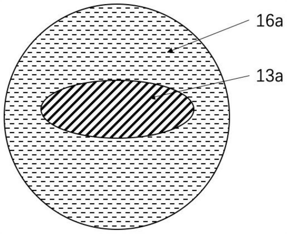
[0034] like figure 2 As shown, in Embodiment 1, the patterned piezoelectric oscillator stack portion 13 is elliptical; in the acoustic reflection structure, the high acoustic impedance layer is Mo, and the low acoustic impedance layer is SiO 2 .
Embodiment 2
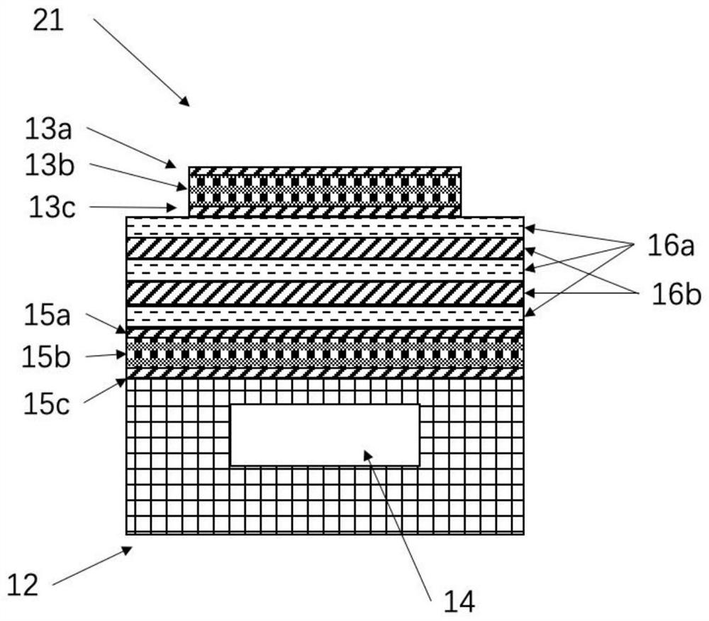
[0036] like Figure 3-4 As shown, the second tunable fixed-mounted BAW resonator 21 provided in the second embodiment includes a substrate 12 , a piezoelectric oscillation stack 13 , an acoustic reflection structure 16 and a tuning structure 15 . There is a cavity 14 in the middle of the substrate 12; the tuning structure 15 sequentially includes a first electrode 15a, a piezoelectric layer 15b and a second electrode 15c from top to bottom; the acoustic reflection layer includes a low acoustic impedance layer SiO from top to bottom 2 16a, a high acoustic impedance layer Mo16b; the piezoelectric oscillation stack 13 sequentially includes from bottom to top: a top electrode 13a, a piezoelectric layer 13b and a bottom electrode 13c.
[0037] like Figure 4 As shown, in the second embodiment, the patterned piezoelectric oscillator stack portion 13 is an irregular pentagon; in the acoustic reflection structure, the high acoustic impedance layer is Mo, and the low acoustic impedanc...
Embodiment 3
[0039] like Figure 5-6 As shown, the third tunable fixed-mounted BAW resonator 31 provided in Embodiment 3 includes a substrate 12 , a piezoelectric oscillation stack 13 , an acoustic reflection structure 16 and a tuning structure 15 . There is a cavity 14 in the middle of the substrate 11; the tuning structure 15 sequentially includes from top to bottom: a first electrode 15a, a piezoelectric layer 15b and a second electrode 15c; the acoustic reflection layer includes from top to bottom: a low acoustic impedance layer SiO 2 16a, a high acoustic impedance layer W16c; the piezoelectric oscillation stack 13 sequentially includes from bottom to top: a top electrode 13a, a piezoelectric layer 13b and a bottom electrode 13c.
[0040] like Image 6 As shown, in Embodiment 3, the patterned piezoelectric oscillator stack portion 13 is elliptical; in the acoustic reflection structure, the high acoustic impedance layer is W, and the low acoustic impedance layer is SiO 2 .
PUM
| Property | Measurement | Unit |
|---|---|---|
| Thickness | aaaaa | aaaaa |
| Thickness | aaaaa | aaaaa |
Abstract
Description
Claims
Application Information


