

Netlist-level circuit area optimization method based on AND gate inverter diagram and storage medium
An area optimization, level circuit technology, applied in the field of netlist level circuit area optimization method and storage medium based on the AND gate inverter diagram, can solve the problems of non-universality, reduce circuit structure redundancy, memory reduction, the effect of reducing the area of the circuit structure
- Summary
- Abstract
- Description
- Claims
- Application Information
AI Technical Summary
Problems solved by technology
Method used
Image

Examples
Embodiment 1
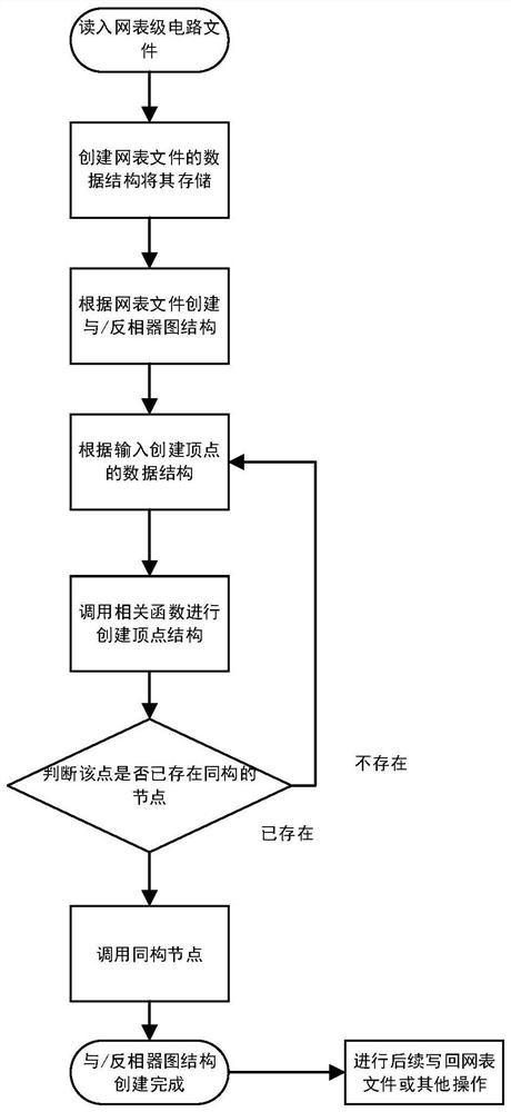
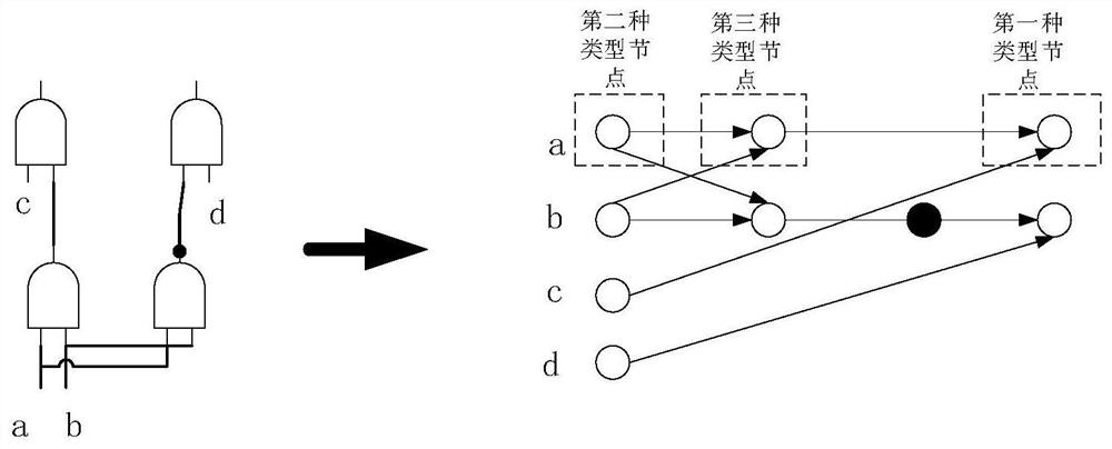
[0037] At present, for the optimization and improvement of netlist-level circuits, most of the related technologies are to preprocess the netlist-level circuits and correspond to the next specific operation process, and use corresponding algorithms to optimize the cost of this operation process, such as in When performing netlist-level circuit segmentation, it is often optimized by optimizing the time and accuracy of the segmentation algorithm after converting the netlist-level circuit into a hypergraph form or other forms. Although these methods can achieve optimized results , but they are all optimizing the operation of the circuit for a certain purpose, and cannot be optimized above the level of the circuit itself; secondly, for some small circuit designs, people may use Boolean algebra such as Karnaugh maps, or other The simplification method is used to perform mathematical calculations to achieve the purpose of reducing circuit structure redundancy and circuit area. This m...
Embodiment 2
[0065] The present invention also provides a computer-readable storage medium, where a computer program is stored in the computer-readable storage medium, and when the computer program is executed by a processor, the steps of the first embodiment above are implemented.
[0066] Generally, the computer-readable storage medium can be placed in a computer device, see Figure 6, the computer device may include units or modules such as a processor, a communication interface, a computer-readable storage medium, and a communication bus, wherein the processor, the communication interface, and the memory complete mutual communication through the communication bus,
[0067] Computer-readable storage medium for storing computer programs;
[0068] When the processor is used to execute the program stored on the computer-readable storage medium, the following steps are implemented:
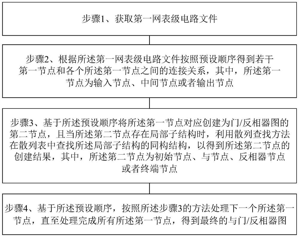
[0069] Step 1, obtaining the first netlist-level circuit file;
[0070] Step 2. According to the first net...
PUM
 Abstract
Description
Claims
Application Information