

Semiconductor structure and preparation method thereof
A semiconductor and trench technology, which is applied in semiconductor/solid-state device manufacturing, semiconductor devices, semiconductor/solid-state device components, etc., can solve problems such as increased aspect ratio and metal plugs that tend to have gaps or holes
- Summary
- Abstract
- Description
- Claims
- Application Information
AI Technical Summary
Problems solved by technology
Method used
Image

Examples
Embodiment Construction
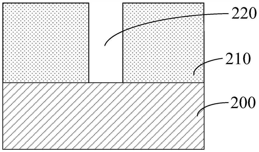
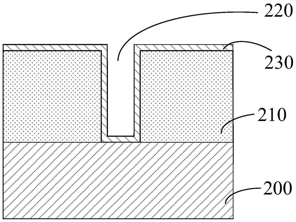
[0036] In order to facilitate the understanding of the present invention, the present invention will be described more fully below with reference to the associated drawings. A preferred embodiment of the invention is shown in the drawings. However, the present invention can be embodied in many different forms and is not limited to the embodiments described herein. Rather, these embodiments are provided so that the disclosure of the present invention will be thorough and complete. It should be noted that the terms "forming", "converting", "filling" and similar expressions used herein are for illustrative purposes only.
[0037] Unless otherwise defined, all technical and scientific terms used herein have the same meaning as commonly understood by one of ordinary skill in the technical field of the invention. The terms used herein in the description of the present invention are for the purpose of describing specific embodiments only, and are not intended to limit the present i...
PUM
| Property | Measurement | Unit |
|---|---|---|
| thickness | aaaaa | aaaaa |
Abstract
Description
Claims
Application Information