Miniature LED mass transfer method and device based on high-speed scanning laser transfer printing

A technology of laser transfer printing and high-speed scanning, which is applied in the manufacture of semiconductor devices, electrical components, semiconductor/solid-state devices, etc., can solve the problems of yield and efficiency, and achieve the elimination of thermal damage, low power consumption, and high transfer rate Effect

Active Publication Date: 2021-05-07
WUHAN UNIV OF TECH
View PDF4 Cites 8 Cited by
  • Summary
  • Abstract
  • Description
  • Claims
  • Application Information

AI Technical Summary

Problems solved by technology

[0008] In order to solve the problems of yield and efficiency in the existing Micro-LED mass transfer process, the present invention provides a micro-LED mass transfer method and device based on high-speed scanning laser transfer printing

Method used


Image

  • Miniature LED mass transfer method and device based on high-speed scanning laser transfer printing
  • Miniature LED mass transfer method and device based on high-speed scanning laser transfer printing
  • Miniature LED mass transfer method and device based on high-speed scanning laser transfer printing

Examples


Embodiment Construction

[0038] In order to make the purpose, technical solutions and advantages of the embodiments of the present invention clearer, the technical solutions in the embodiments of the present invention will be clearly and completely described below in conjunction with the drawings in the embodiments of the present invention. Obviously, the described embodiments It is a part of embodiments of the present invention, but not all embodiments. It should be understood that the specific embodiments described here are only used to explain the present invention, not to limit the present invention. Based on the embodiments of the present invention, all other embodiments obtained by persons of ordinary skill in the art without making creative efforts belong to the protection scope of the present invention.

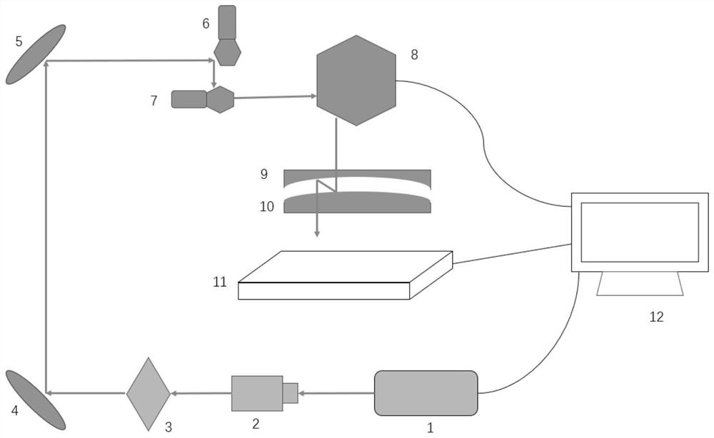
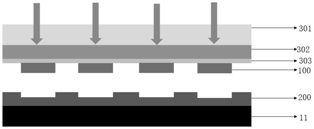
[0039] Such as Figure 1-Figure 4 As shown, a method of mass transfer of micro-LEDs based on high-speed scanning laser transfer printing includes the following steps:

[0040] S1. Prepare t...


PUM

PropertyMeasurementUnit
Thicknessaaaaaaaaaa
Thicknessaaaaaaaaaa

Abstract

The invention discloses a miniature LED mass transfer method and device based on high-speed scanning laser transfer printing. The method comprises the following steps that: S1, a miniature LED chip, a receiving substrate, a transmitting substrate and a femtosecond laser are prepared, wherein the transmitting substrate comprises a transparent substrate, a polyimide layer and a bonding layer; S2, the miniature LED chip is adhered to the bonding layer, and then the transmitting substrate is arranged right above the receiving substrate; and S3, the femtosecond laser is started, femtosecond laser is focused at the junction of the transparent substrate and the polyimide layer to form a hot air cavity, hot air in the hot air cavity downwards extrudes the polyimide layer and the bonding layer, and the miniature LED chip is pushed to the receiving substrate and falls into the position, where the miniature LED chip is to be received, of the receiving substrate. According to the miniature LED mass transfer method and device based on the high-speed scanning laser transfer printing, the polyimide shallow layer area is ablated through the ultraviolet femtosecond laser, the generated high-pressure gas pushes the Micro-LED chip layer to the receiving substrate, and therefore, the transfer rate is high, and no damage is caused to devices.

Description

technical field [0001] The invention belongs to the technical field of semiconductor optoelectronics, and in particular relates to a method and device for mass transfer of micro LEDs based on high-speed scanning laser transfer printing. Background technique [0002] Micro-LED technology, that is, LED miniaturization and matrixing technology, integrates a high-density micro-sized LED array on a chip, and the pixel size is below 100 microns. Micro-LED technology is a new self-luminous display technology. Compared with traditional LCD, OLED, etc., Micro LED has the characteristics of low power consumption, fast response, long life, and high light efficiency. As the display size increases, it is necessary to transfer LED chips with a size of millions or even tens of millions of microns, which cannot be met by traditional transfer processes. [0003] Various mass transfer technologies of Micro-LED can be roughly classified into the following categories at this stage. [0004] 1...

Claims


Application Information

Patent Timeline
IPC IPC(8): H01L33/00H01L21/67
CPCH01L33/0095H01L21/67144H01L2224/95001
Inventor 王学文冯宇哲孙楷理
Owner WUHAN UNIV OF TECH
Why Eureka
Try Eureka