

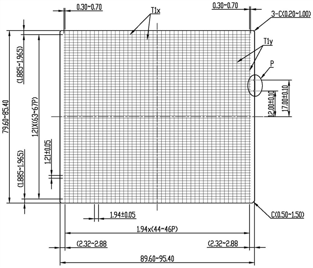
A large size ceramic substrate
A ceramic substrate, large-scale technology, applied in the direction of resistance manufacturing, resistors, electrical components, etc., can solve the problems of low production efficiency, achieve the effects of increasing production efficiency, improving warpage, and controlling warpage
- Summary
- Abstract
- Description
- Claims
- Application Information
AI Technical Summary
Problems solved by technology
Method used
Image

Examples
Embodiment 1
[0083] 1. Put the alumina powder and the flux into the ball mill in a certain proportion, wherein the proportion of the alumina powder in the solid phase component is 95wt%, and the flux component is SiO 2 -MgO-CaO, the ratio of which is 1.5:0.8:0.4, and the addition amount is 5wt%. Then add additives and solvent into the ball mill to prepare slurry. The additives mainly include the binder PVB and the plasticizer DBP. The addition amount of the additives is relative to 100wt% of the solid phase component. The addition amount of the binder PVB is 5wt% and the plasticizer DBP is 5wt%. The amount of the solvent is 50% of the mass of the powder (alumina powder and flux), and the mass ratio of toluene and isopropanol in the solvent is 6:11.
[0084] 2. Casting molding: The slurry prepared above is uniformly coated on a smooth transmission PET release film through the casting nozzle, and dried in an oven to form a green body with a certain thickness, density and uniformity.
[008...
Embodiment 2
[0091] The only difference between this example and Example 1 is that the addition amount of the binder PVB is 6 wt %, and the rest is the same as that of Example 1.
Embodiment 3
[0093] The only difference between this example and Example 1 is that the addition amount of the binder PVB is 8 wt %, and the rest is the same as that of Example 1.
PUM
| Property | Measurement | Unit |
|---|---|---|
| depth | aaaaa | aaaaa |
| depth | aaaaa | aaaaa |
| length | aaaaa | aaaaa |
Abstract
Description
Claims
Application Information