Semiconductor processing equipment

A technology for processing equipment and semiconductors, which is used in semiconductor/solid-state device manufacturing, semiconductor/solid-state device testing/measurement, electrical components, etc., and can solve problems such as unsatisfactory process effects and inability to respond quickly to pressure changes.

Pending Publication Date: 2021-05-28
BEIJING NAURA MICROELECTRONICS EQUIP CO LTD
View PDF0 Cites 4 Cited by
  • Summary
  • Abstract
  • Description
  • Claims
  • Application Information

AI Technical Summary

Problems solved by technology

[0004] The present application discloses a semiconductor processing equipment to solve the problem that the process effect i

Method used


Image

  • Semiconductor processing equipment
  • Semiconductor processing equipment
  • Semiconductor processing equipment

Examples


Embodiment Construction

[0024] In order to make the purpose, technical solution and advantages of the present application clearer, the technical solution of the present application will be clearly and completely described below in conjunction with specific embodiments of the present application and corresponding drawings. Apparently, the described embodiments are only some of the embodiments of this application, not all of them. Based on the embodiments in this application, all other embodiments obtained by persons of ordinary skill in the art without making creative efforts belong to the scope of protection of this application.

[0025] The technical solutions disclosed in various embodiments of the present application will be described in detail below with reference to the accompanying drawings.

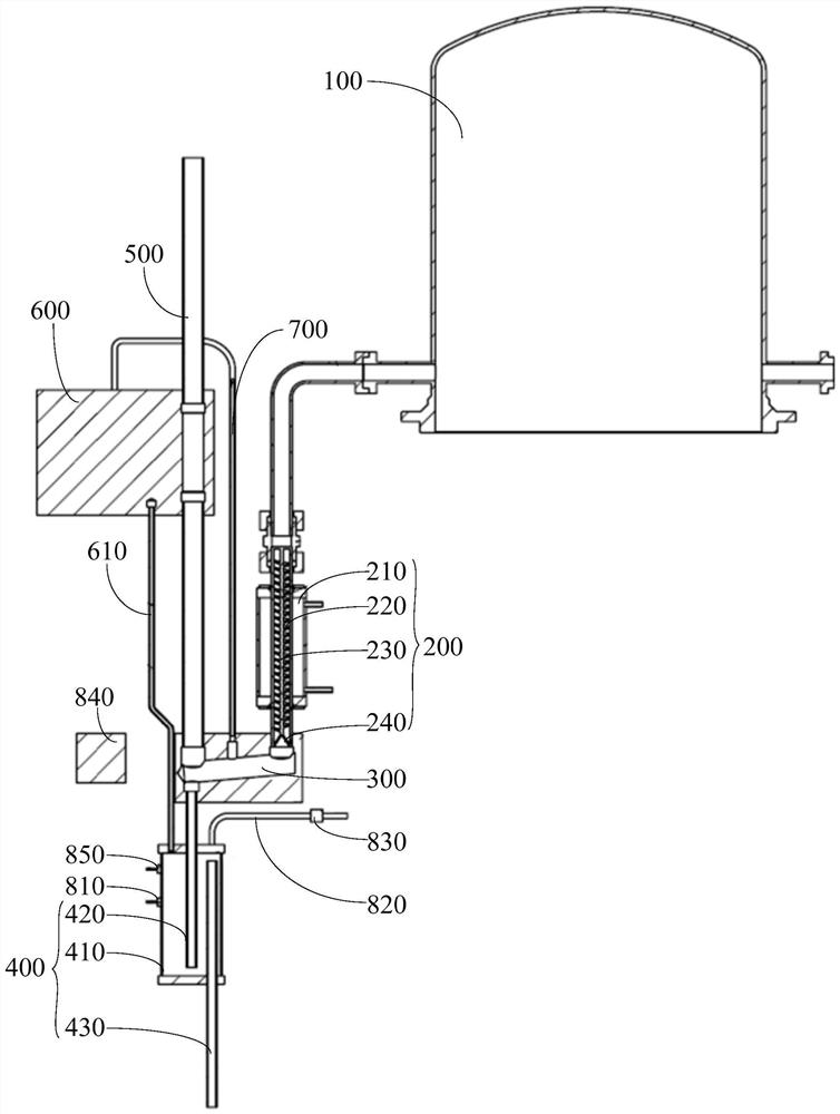
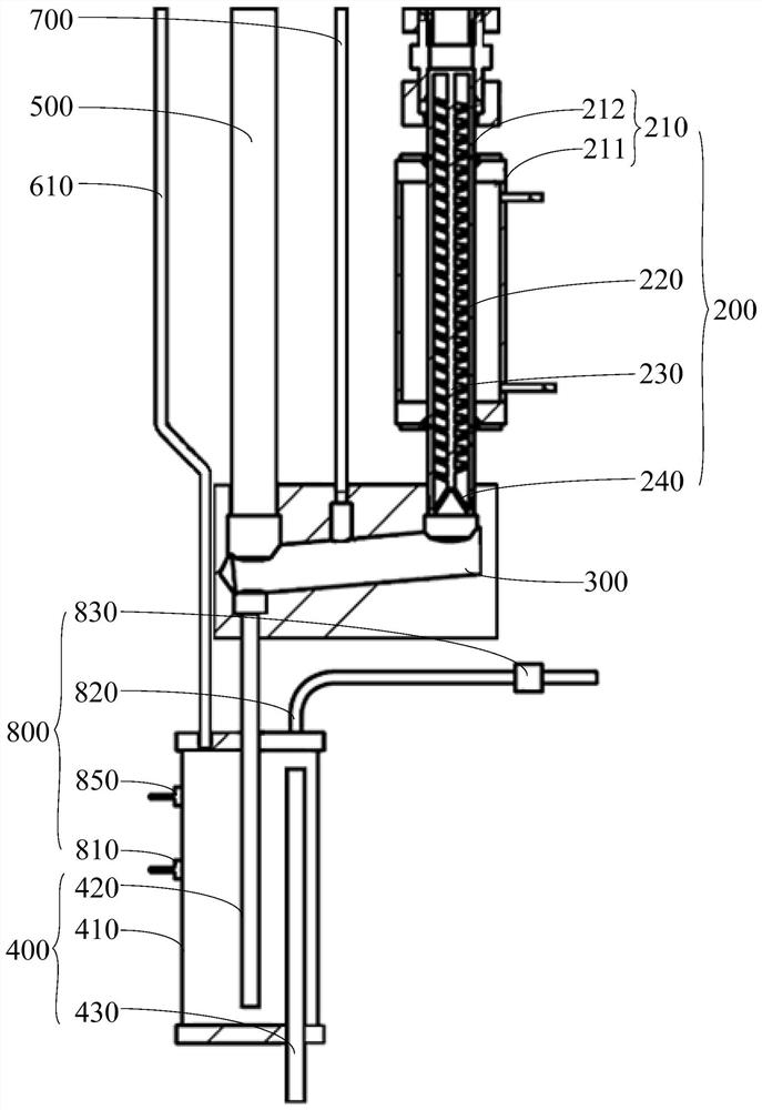
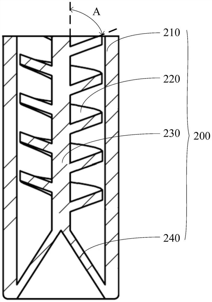
[0026] Please refer to Figure 1 to Figure 3 , the embodiment of the present application discloses a semiconductor processing equipment, and the disclosed semiconductor processing equipment includes a re...


PUM


Abstract

The invention discloses semiconductor processing equipment, which comprises a reaction chamber (100), a condenser (200), a switching part (300) and a water box (400), wherein the reaction chamber (100), the condenser (200), the switching part (300) and the water box (400) are communicated in sequence, the condenser (200) comprises a pipe body (210) and a spiral damping sheet (220) arranged in the pipe body (210), the spiral damping sheet (220) is provided with a spiral face facing the air inlet end opening of the pipe body (210), and the included angle (A) between the spiral face and the axis direction of the pipe body (210) is smaller than 90 degrees. According to the scheme, the problem that the process effect is not ideal due to the fact that semiconductor process equipment cannot quickly respond to pressure changes can be solved.

Description

technical field [0001] The present application relates to the technical field of semiconductor processing, in particular to a semiconductor processing equipment. Background technique [0002] The wet oxygen oxidation process is involved in the processing of semiconductors, and the wet oxygen oxidation process is widely used due to its advantages of fast film formation rate. [0003] In the related art, during the wet oxygen oxidation process, the gas discharged from the reaction chamber of the corresponding semiconductor processing equipment will be condensed by the condenser, and finally transported to the next process. However, the condenser has a large resistance to the gas, so that the pressure change in the reaction chamber cannot be detected by the pressure detection equipment relatively quickly, which leads to the inability of the semiconductor process equipment to respond relatively quickly according to the pressure change in the reaction chamber. Ultimately, it wil...

Claims


Application Information

Patent Timeline
IPC IPC(8): H01L21/67H01L21/02H01L21/66
CPCH01L21/0223H01L21/67253H01L22/10
Inventor 石磊王立卡
Owner BEIJING NAURA MICROELECTRONICS EQUIP CO LTD
Why Eureka
Try Eureka