

A kind of transparent conductive film and preparation method thereof
A technology of transparent conductive film and conductive layer, which is applied to equipment for manufacturing conductive/semiconductive layers, cable/conductor manufacturing, conductive layers on insulating carriers, etc., which can solve uneven stress distribution and cracking of conductive oxide layers , warping and other issues, to achieve good performance, improve stability, not easy to crack or warp
- Summary
- Abstract
- Description
- Claims
- Application Information
AI Technical Summary
Problems solved by technology
Method used
Image

Examples
preparation example Construction
[0044] The present invention also provides a method for preparing a transparent conductive film, comprising:
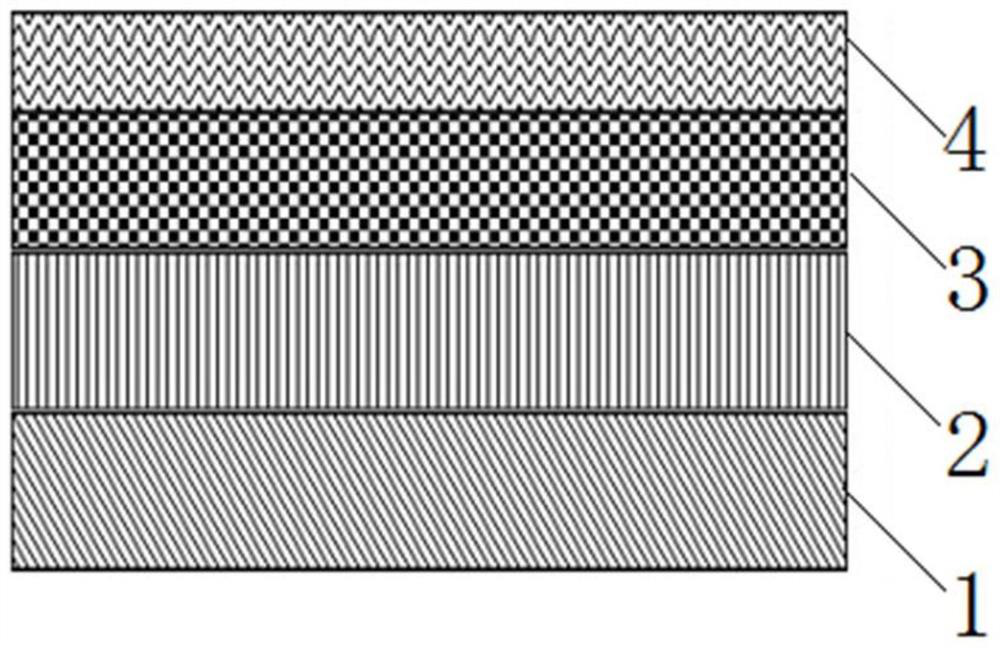
[0045] Prepare the first conductive layer on the surface of the transparent substrate:
[0046] A layer of conductive oxide is deposited on the surface of the transparent substrate, and then annealed to obtain a first conductive layer, wherein the annealing temperature is 120-170°C, and the annealing time is 20-40min;
[0047] Prepare a second conductive layer on the surface of the first conductive layer:
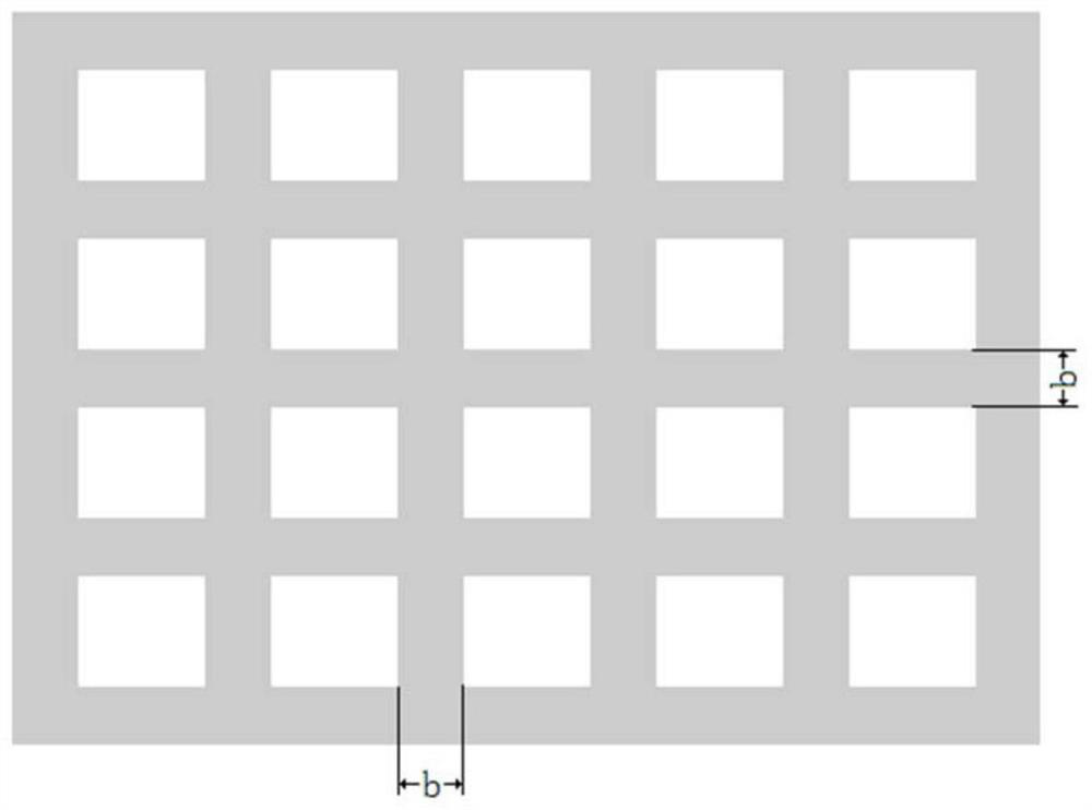
[0048] coating, depositing or printing a conductive material on the surface of the first conductive layer to form a second conductive layer containing a pattern;
[0049] Prepare a third conductive layer on the surface of the second conductive layer:
[0050] A layer of conductive oxide is deposited on the surface of the second conductive layer to form a third conductive layer.
[0051] In the present invention, the first conductive layer containing the conducti...
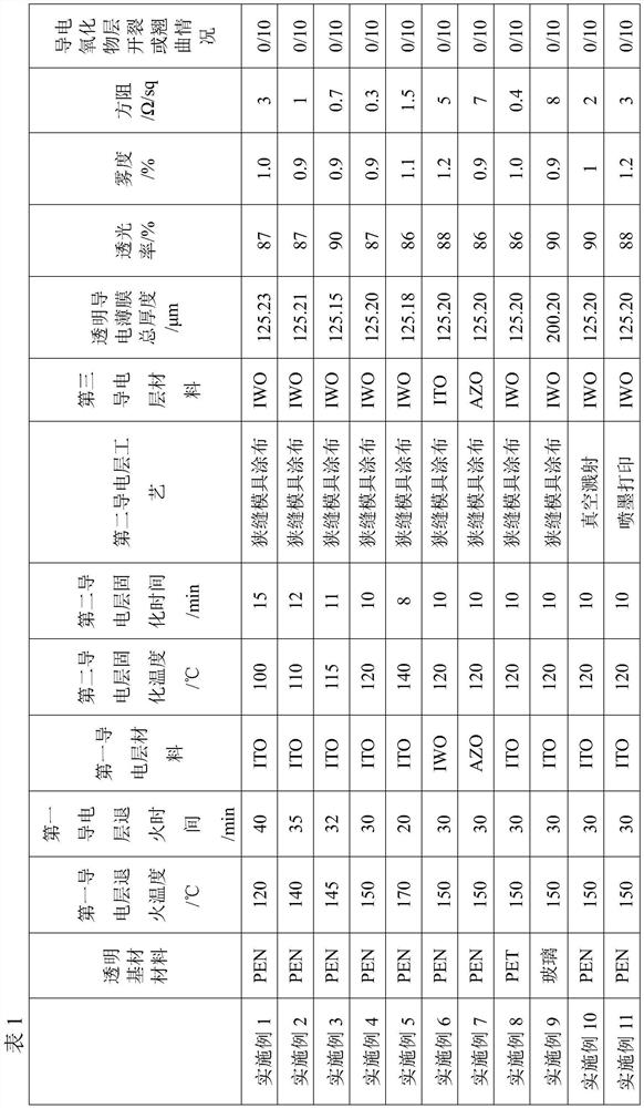
Embodiment 1
[0084]
[0085] The first conductive layer of ITO was prepared on the surface of a PEN transparent substrate with a thickness of 125 μm by vacuum magnetron sputtering, and then annealed at a temperature of 120° C. and an annealing time of 40 min. The thickness of the first conductive layer was 100 nm.
[0086]
[0087] After the nano-silver wires and anhydrous ethanol are mixed and dispersed uniformly, a nano-metal wire paste with a concentration of 8 mg / ml is obtained. The nanowires are 20 μm in length and 30 nm in diameter.
[0088]The nano metal wire slurry was coated on the surface of the first conductive layer through a slit coating die, and the second conductive layer was formed after curing; wherein the curing temperature was 100° C. and the curing time was 15 minutes. The thickness of the second conductive layer is 80 nm, that is, the thickness of the nano-silver wire layer, the line width of the nano-silver wire is 20 μm, and the line spacing is 500 μm.
[0089]...
Embodiment 2
[0092] Except in , the annealing temperature of the first conductive layer is 140°C, the annealing time is 35min, and the thickness of the first conductive layer is 50 nm; in , the nano metal The concentration of the wire paste is 8mg / ml, the curing temperature is 110°C, the curing time is 12min, and the thickness of the second conductive layer is 120nm; Except that the layer thickness was 40 nm, the rest was the same as that of Example 1.
PUM
| Property | Measurement | Unit |
|---|---|---|
| length | aaaaa | aaaaa |
| diameter | aaaaa | aaaaa |
| width | aaaaa | aaaaa |
Abstract
Description
Claims
Application Information