Semiconductor etching equipment and silicon carbide wafer etching method

A technology of etching equipment and semiconductors, applied in chemical instruments and methods, semiconductor/solid-state device manufacturing, crystal growth, etc., can solve problems such as tip discharge and fragile devices

Active Publication Date: 2021-06-08
BEIJING NAURA MICROELECTRONICS EQUIP CO LTD
View PDF5 Cites 1 Cited by
  • Summary
  • Abstract
  • Description
  • Claims
  • Application Information

AI Technical Summary

Problems solved by technology

[0004] The invention discloses a semiconductor etching device and an etching method for a silicon carbide wafer, in order to solve the problem that when etching a silicon carbide w

Method used


Image

  • Semiconductor etching equipment and silicon carbide wafer etching method
  • Semiconductor etching equipment and silicon carbide wafer etching method
  • Semiconductor etching equipment and silicon carbide wafer etching method

Examples


Embodiment Construction

[0026] In order to make the purpose, technical solution and advantages of the present invention clearer, the technical solution of the present invention will be clearly and completely described below in conjunction with specific embodiments of the present invention and corresponding drawings. Apparently, the described embodiments are only some of the embodiments of the present invention, but not all of them. Based on the embodiments of the present invention, all other embodiments obtained by persons of ordinary skill in the art without making creative efforts belong to the protection scope of the present invention.

[0027] The technical solutions disclosed by various embodiments of the present invention will be described in detail below in conjunction with the accompanying drawings.

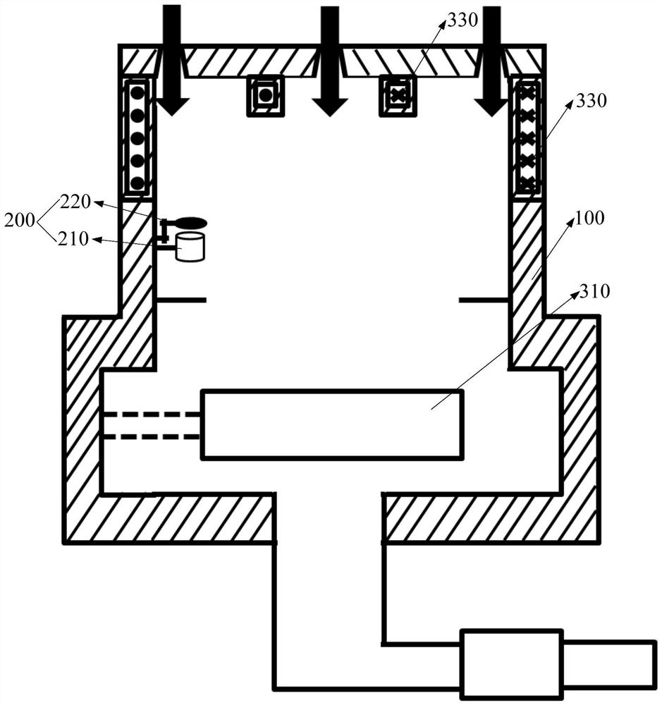
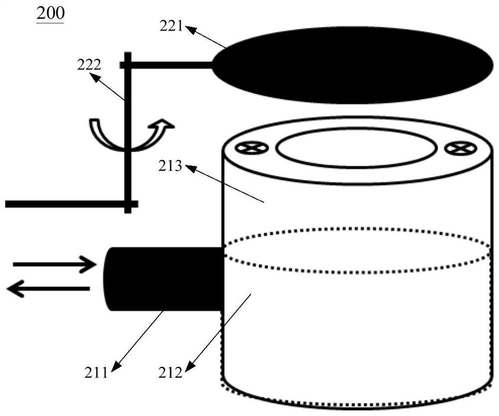
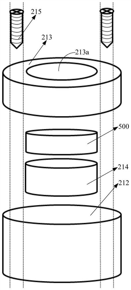
[0028] like Figure 1-Figure 4 As shown, the embodiment of the present application discloses a semiconductor etching equipment, which includes a process chamber 100, a magnetron sputtering asse...


PUM


Abstract

The invention discloses a semiconductor etching device and a silicon carbide wafer etching method. The semiconductor etching device comprises a process chamber, the process chamber is internally provided with a magnetron sputtering assembly, and the magnetron sputtering assembly is installed on the side wall of the process chamber and located above a bearing part used for bearing the wafer in the process chamber; and the magnetron sputtering assembly comprises a base assembly and a shielding assembly, the base assembly is used for fixing a target material and attracting plasma to bombard the target material, and the shielding assembly can rotate and is used for selectively shielding the target material. By adopting the semiconductor etching device to etch a silicon carbide wafer, the problem that a device is easy to damage due to a point discharge phenomenon caused by the fact that the side wall and the bottom surface of a formed etching structure are almost vertical can be solved.

Description

technical field [0001] The invention relates to the technical field of semiconductor processing, in particular to a semiconductor etching device and an etching method for a silicon carbide wafer. Background technique [0002] As the third-generation wide-bandgap semiconductor material, silicon carbide (SiC) material has a series of advantages such as large bandgap width, high thermal conductivity, high breakdown electric field strength, high saturated electron drift speed and ability to withstand extreme environmental changes, making SiC Materials have great application potential in high temperature, high frequency, high power, optoelectronics and radiation resistance. At present, silicon carbide materials are mainly used in the preparation of electronic devices. [0003] Silicon carbide material has high hardness and very stable chemical properties. Generally speaking, dry etching is used to etch silicon carbide wafers. Generally speaking, in the process of etching silicon...

Claims


Application Information

Patent Timeline
IPC IPC(8): C30B33/12C30B29/36C23C14/35C23C14/04H01L21/04H01L21/67
CPCC30B33/12C30B29/36C23C14/35C23C14/042H01L21/67069H01L21/0475H01L21/045
Inventor 林源为谭晓宇
Owner BEIJING NAURA MICROELECTRONICS EQUIP CO LTD
Why Eureka
Try Eureka