Low-noise amplifier chip of W-band filterable structure

A technology of low-noise amplifier and filter structure, applied in the direction of improving amplifiers to reduce the influence of noise, etc., can solve the problems of inconvenient miniaturization design, LC filter circuit area and high cost, reduce area, increase throughput, and meet the needs of The effect of miniaturization

Pending Publication Date: 2021-06-11
CHENGDU UNIVERSITY OF TECHNOLOGY
View PDF0 Cites 1 Cited by
  • Summary
  • Abstract
  • Description
  • Claims
  • Application Information

AI Technical Summary

Problems solved by technology

[0005] Among the above-mentioned low-noise amplifier chips, most of the filterable chips use LC resonant circuits, but the circuit area and cost of LC filtering are relatively high
It is not convenient for miniaturization design in W band

Method used


Image

  • Low-noise amplifier chip of W-band filterable structure
  • Low-noise amplifier chip of W-band filterable structure
  • Low-noise amplifier chip of W-band filterable structure

Examples


Embodiment Construction

[0023] In order to make the purpose, technical solution and advantages of the present invention clearer, the technical solution of the present invention will be described in detail below. Apparently, the described embodiments are only some of the embodiments of the present invention, but not all of them. Based on the embodiments of the present invention, all other implementations obtained by persons of ordinary skill in the art without making creative efforts fall within the protection scope of the present invention.

[0024] A specific W-band filterable low noise amplifier chip provided in the embodiment of the present application will be described below with reference to the accompanying drawings.

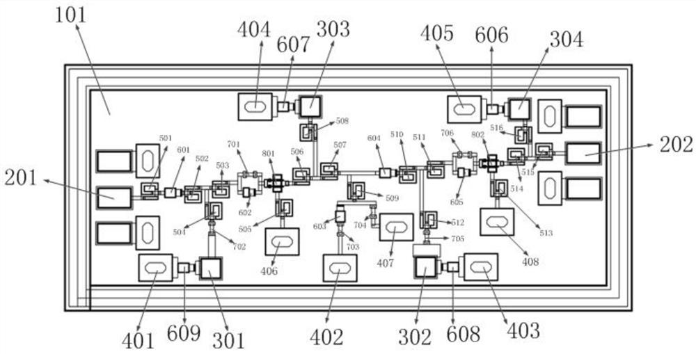
[0025] figure 1 It is the layout of the low noise amplifier chip of the W-band controllable filter structure provided in the embodiment of the present application. Including a GaAs substrate 101, the GaAs substrate 101 includes a first-stage amplifying circuit and a second-stag...


PUM

PropertyMeasurementUnit
thicknessaaaaaaaaaa

Abstract

The invention designs a low-noise amplifier chip of a W-band filterable structure, and the chip comprises a GaAs substrate; a first-stage amplification circuit and a second-stage amplification circuit are arranged on the GaAs substrate; the first-stage amplification circuit and the second-stage amplification circuit are cascaded, and the first-stage amplification circuit comprises an input GSG (Ground-Single-Ground), an input matching circuit, a T-type matching circuit, a gate bias circuit, a resistor-capacitor parallel filter circuit, a first GaAs FET tube group, a GaAs FET tube group source series inductance grounding structure, the other T-type matching circuit and a drain bias circuit from the left to the right; The second-stage amplification circuit is similar to the first-stage amplification circuit. And the first-stage amplification circuit is connected with the second-stage amplification circuit through an inter-stage matching circuit. The invention aims to overcome the defects in the prior art, provides a low-noise amplifier chip of a W-band filterable structure, and provides an RC parallel structure compared with a conventional chip structure, so low-frequency signals can be well inhibited, and the filtering effect is achieved.

Description

technical field [0001] The invention relates to the technical field of radio frequency low-noise power amplifiers, in particular to a low-noise amplifier chip with a W-band filterable structure. [0002] technical background [0003] In recent years, wireless communication technology has made unprecedented progress, and as the integration of devices is getting higher and higher, the expansion to higher frequencies has become the trend of the times. RF Low Noise Amplifier (Low Noise Amplifier), as the first active stage in the front end of a wireless receiver, largely determines the performance of the receiving system, and is widely used in W-band systems involving millimeter-wave imaging , radar, communications and other fields. [0004] In the W-band transceiver system, there will be more or less spurious and unwanted signals in the system during the debugging process. Therefore, the research on low-noise amplifiers that can filter is of great significance. [0005] Among ...

Claims


Application Information

Patent Timeline
Patent Type & Authority Applications(China)
IPC IPC(8): H03F1/26
CPCH03F1/26
Inventor 牟聪刘强孟一宁
Owner CHENGDU UNIVERSITY OF TECHNOLOGY
Why Eureka
Try Eureka