Full-automatic light-emitting diode die bonding equipment and process

A light-emitting diode, fully automatic technology, applied in electrical components, circuits, semiconductor devices, etc., can solve the problems that electromagnets cannot be sucked, separated and transported, have no transport, and the feeding device cannot be separated, etc., to improve product quality and Work efficiency, reduce the drop height, avoid the effect of friction

Active Publication Date: 2021-06-18
宇之亮电子(深圳)有限公司
View PDF5 Cites 0 Cited by
  • Summary
  • Abstract
  • Description
  • Claims
  • Application Information

AI Technical Summary

Problems solved by technology

[0004] In view of the above-mentioned related technologies, the inventor believes that since the LED bracket also includes copper brackets, aluminum brackets, and ceramic brackets, the electromagnet cannot fail to absorb and separate the copper brackets, aluminum brackets, and ceramic brackets. The feeding device in the LED die bonder has the defect that it cannot be separated and handles non-magnetic brackets.

Method used


Image

  • Full-automatic light-emitting diode die bonding equipment and process
  • Full-automatic light-emitting diode die bonding equipment and process
  • Full-automatic light-emitting diode die bonding equipment and process

Examples


Embodiment Construction

[0041] The following is attached Figure 1-5 The application is described in further detail.

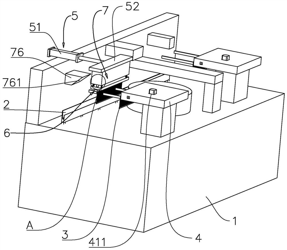
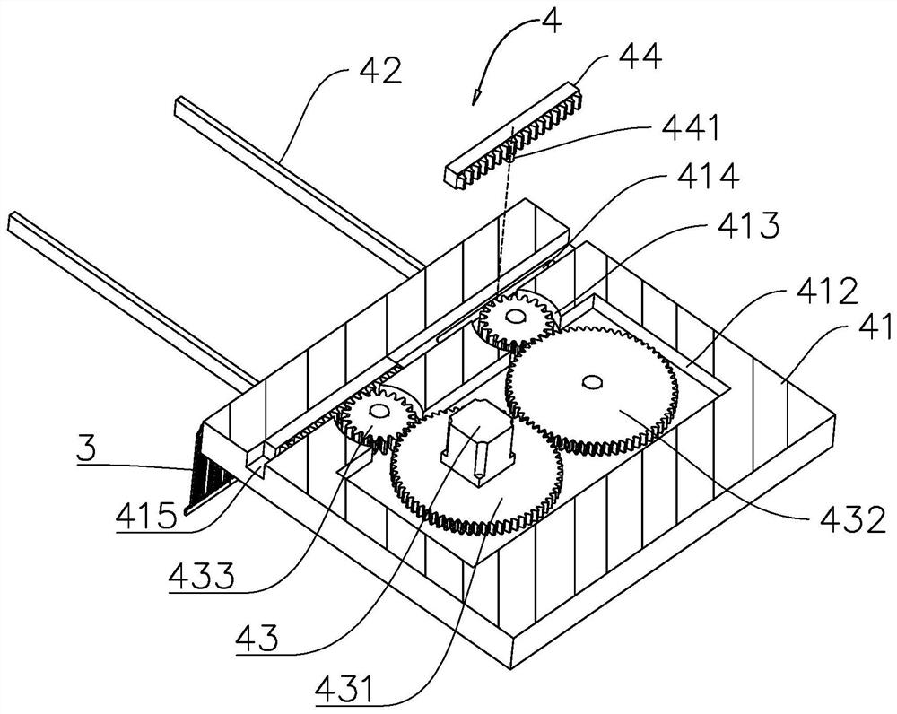
[0042] The embodiment of the present application discloses a fully automatic light-emitting diode crystal bonding equipment. refer to figure 1 and figure 2 , the fully automatic light-emitting diode crystal-bonding equipment includes a machine base 1, the machine base 1 is vertically arranged, the upper end of the machine base 1 is provided with a flow channel 2, and one side of the flow channel 2 is provided with a material fork 4 for placing several brackets 3, and the material The fork 4 includes a chassis 41 and two parallel supporting rods 42 arranged on the chassis 41, wherein the chassis 41 is horizontally arranged and installed on the upper end surface of the machine base 1, and the supporting rods 42 are located on the side of the chassis 41 close to the flow channel 2 , the two supporting rods 42 pass through the bracket 3 so that the bracket 3 overlaps the two supporti...


PUM


Abstract

The invention relates to the field of semiconductor packaging equipment, and concretely relates to full-automatic light-emitting diode die bonding equipment and process. The equipment comprises a machine base, a runner is arranged on the machine base, and a material fork used for placing a plurality of supports is arranged on one side of the runner; the machine base is provided with a translation structure used for pushing a support closest to the runner to move towards the position where the runner is located, the translation structure is provided with a clamping structure used for clamping the support, and the clamping structure is located above the support; and the clamping structure is further provided with a downward moving structure used for reducing the vertical displacement between one support clamped by the clamping structure and the runner, and the downward moving structure is connected between the clamping structure and the horizontal moving structure. The equipment and the process have the advantages that an LED die bonder can be separated, and the support without magnetism can be carried.

Description

technical field [0001] The present application relates to the field of semiconductor packaging equipment, in particular to a fully automatic light-emitting diode crystal bonding equipment and process. Background technique [0002] Die bonding is also called Die Bond or die bonding. Die bonding is to bond the chip to the designated area of ​​the bracket through colloid (for LEDs, it is generally conductive glue or insulating glue) to form a thermal path or an electrical path. Wire bonding is a process that provides conditions, so it is necessary to use a die bonder. [0003] LED crystal bonding machine is a professional model for bonding LED products. It is controlled by a computer and equipped with a CCD image sensing system. First, the CCD system scans to determine the correct path, and then enters the set programming program and presses the button easily. The entire workflow can be realized. The workflow includes: first fix the iron bracket that needs to be solidified on...

Claims


Application Information

Patent Timeline
Patent Type & Authority Applications(China)
IPC IPC(8): H01L33/48
CPCH01L33/48H01L2933/0033
Inventor 许明昌
Owner 宇之亮电子(深圳)有限公司
Why Eureka
Try Eureka