Gas sensor

A gas and gas manufacturing technology, which is applied in the fields of instruments, scientific instruments, gaseous chemical plating, etc., can solve the problems of increasing the production cost of the device and increasing the complexity of the process.

Pending Publication Date: 2021-06-18
希奥检测有限公司
View PDF7 Cites 4 Cited by
  • Summary
  • Abstract
  • Description
  • Claims
  • Application Information

AI Technical Summary

Problems solved by technology

This additional deposition of gold or platinum adds to the process complexity and increases the production cost of the device
Also, neither gold nor platinum is CMOS compatible (due to possible deep well formation in the semiconductor bandgap), and the issue of process integration for this layer-behind CMOS is challenging from a cost and supply chain perspective

Method used


Image

  • Gas sensor
  • Gas sensor
  • Gas sensor

Examples


Embodiment Construction

[0135] Some examples of devices are given in the attached drawings.

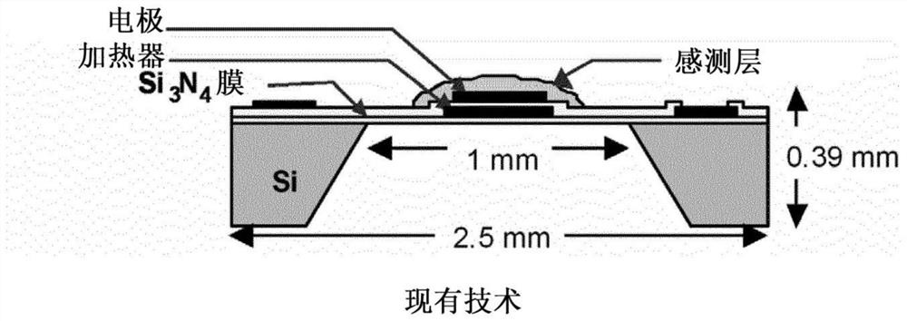
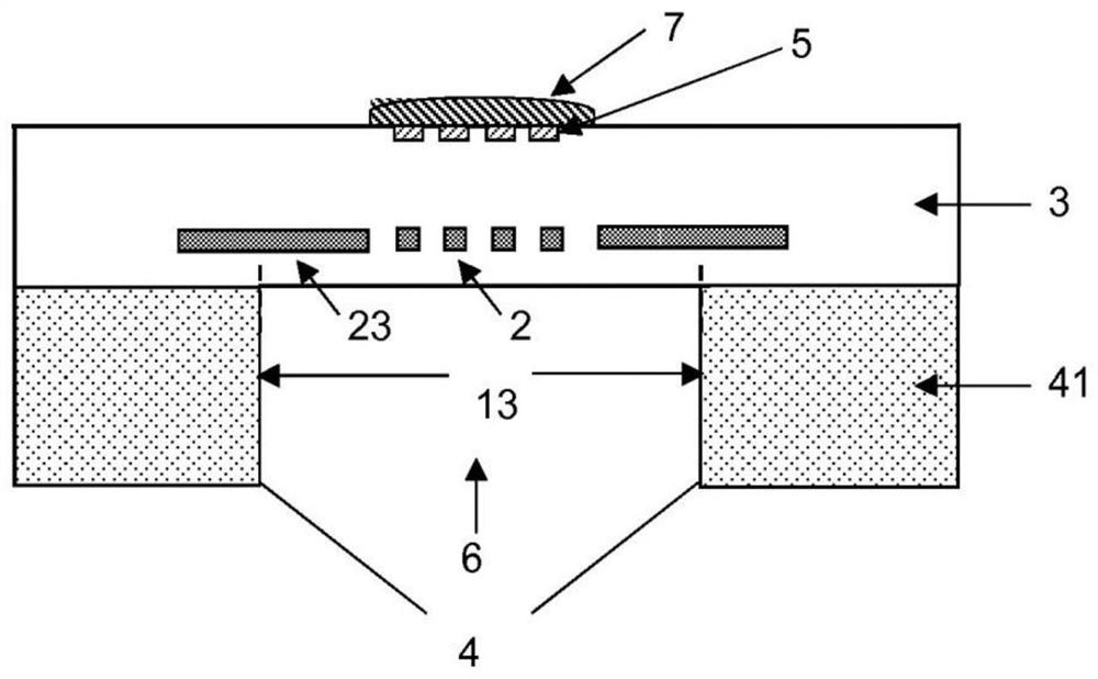
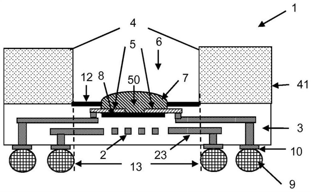
[0136] figure 2 A cross-section of an exemplary gas sensor 1 is shown. The gas sensor 1 comprises a dielectric layer 3 supported by a semiconductor substrate 41 having an etched portion 6 and a substrate portion 4 . In one example, semiconductor substrate 41 can be made of silicon or silicon carbide. The dielectric layer 3 has a dielectric film region or region 13 positioned immediately or directly adjacent or close to the etched portion or cavity 6 of the substrate 41 . In one example, the dielectric layer 3 can be made of a material such as silicon oxide, silicon nitride or a combination thereof. Dielectric film region 13 corresponds to a region (directly) above or below etched portion 6 of dielectric layer 3 . The substrate 41 is etched by DRIE to form an etched portion or cavity 6 .

[0137] The gas sensing material 7 is deposited or grown on the dielectric film 13 . The gas sensing material 7 is ...


PUM

PropertyMeasurementUnit
sizeaaaaaaaaaa
sizeaaaaaaaaaa

Abstract

A gas sensing device comprises: a substrate comprising an etched cavity portion and a substrate portion, a dielectric layer disposed on the substrate, wherein the dielectric layer comprises a dielectric membrane, wherein the dielectric membrane is adjacent to the etched cavity portion of the substrate, a heater located within the dielectric layer; a material for sensing a gas; and one or more polysilicon electrodes coupled with the material for sensing a gas.

Description

technical field [0001] The present disclosure relates to gas sensors, particularly but not limited to micromachined metal oxide gas sensors. Background technique [0002] Metal oxide (MOX) gas sensors are generally based on depositing metal oxide films onto sensing electrodes defined on or within a suitable substrate. Microfabricated MOX gas sensors typically contain a membrane, a heater element within the membrane, and electrodes in direct contact with a metal oxide (MOX) layer. figure 1 A possible structure of a MOX gas sensor is shown in , where a MOX layer is deposited on the membrane and compared with the other by deep reactive ion etching (DRIE) or wet etching (see e.g.: D. Briand et al., "Design and fabrication of high temperature micro -hotplates for drop-coatedgas sensors”, Sensors and Actuators B, 68, pp.223-233, 2000) the cavity formed is opposite. figure 1 The particular example depicted in shows sloped walls that can be achieved by wet etching. Vertical walls...

Claims


Application Information

Patent Timeline
Patent Type & Authority Applications(China)
IPC IPC(8): G01N27/12G01N27/22B81C1/00
CPCG01N27/128G01N27/226G01N27/048G01N27/14G01N27/225G01N33/0036
Inventor 弗洛林·乌德雷亚赛义德·泽尚·艾利
Owner 希奥检测有限公司
Why Eureka
Try Eureka