Wafer test early warning method

A technology for wafer testing and test items, applied in semiconductor/solid-state device testing/measurement, alarms, instruments, etc., can solve the problems of file read and write errors, waste of labor cost and time cost, software stuck, etc. Production efficiency and quality, optimization of design and testing process, effect of saving production cost

Active Publication Date: 2021-06-22
SEMITRONIX
View PDF8 Cites 1 Cited by
  • Summary
  • Abstract
  • Description
  • Claims
  • Application Information

AI Technical Summary

Problems solved by technology

[0004] With the rapid development of integrated circuits, the number of tests in the WAT test process is increasing, which makes the test time very long, and some abnormalities and errors will occur during the test process, such as software content leakage leading to software stuck, file read and write errors , Errors in the interaction process between the test machine software and hardware modules, etc., will affect whether the entire test process can be carried out smoothly
When some abnormal reasons lead to incorrect test results, it is necessary to wait until the current batch of wafer testing is completed to know whether the test results are correct, which greatly wastes labor costs and time costs
In addition, in the existing semiconductor testing, the production process is usually carried out in a constant temperature and humidity workshop. If the technical operator (main user) needs to view the remote test results (without entering the production site), after a wafer test is completed or a batch of finished circuits After the test is completed, the test results can be viewed through the test map, etc.
If there is a production abnormality during the test, it can only be seen after the wafer test is completed, or when the production site is inspected, so it is difficult for the user to deal with the production abnormality in the first place

Method used


Image

  • Wafer test early warning method
  • Wafer test early warning method
  • Wafer test early warning method

Examples


Embodiment 1

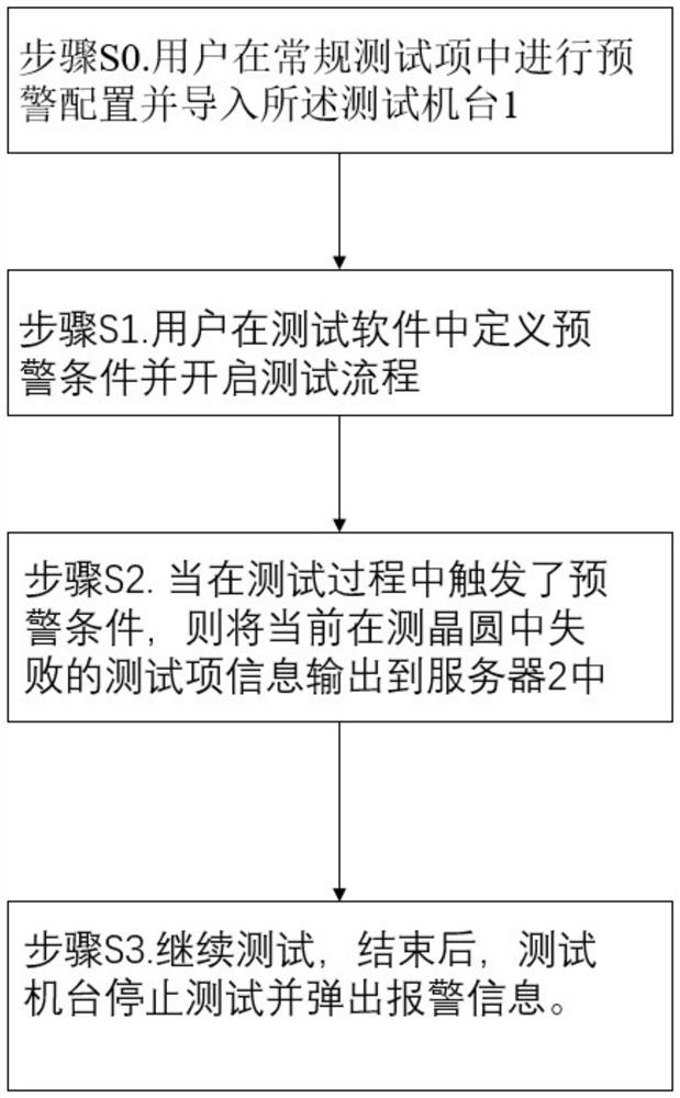
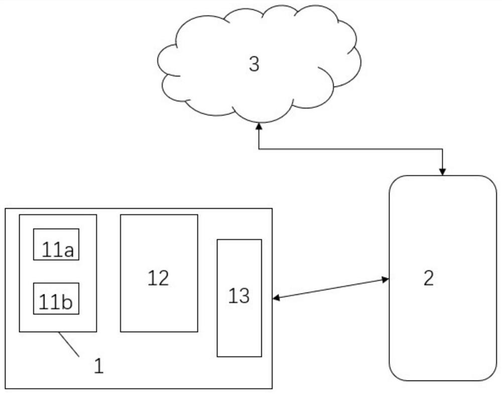
[0024] Such as figure 1 shown, combined with reference figure 2 , in Embodiment 1 of the present invention, the wafer test early warning method specifically includes the following steps: Step S1. The user defines the early warning conditions in the test software and starts the test process; Step S2. The test machine 1 selects the wafer to be tested and starts Test, when an early warning condition is triggered during the test, the test item information that is currently failing in the wafer under test is output to the server 2; Step S3. Continue testing, after the current test of the wafer under test ends, the test The machine stops testing and pops up an alarm message. In this example, if figure 2As shown, the test system includes a test machine 1 and a server 2 , and the test machine 1 includes a test machine 11 , a probe card 12 , and a probe station 13 . The testing machine 11 includes a memory 11a and a processor 11b, and the processor 11b runs the test software on th...

Embodiment 2

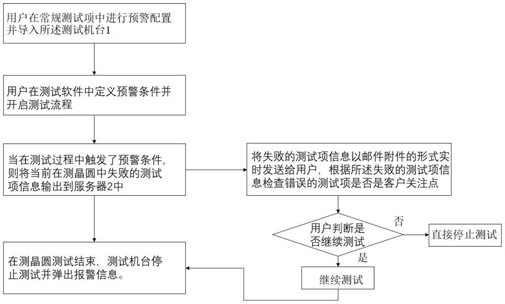
[0027] The difference between this embodiment and the first embodiment is that the server 2 sets a scheduled task plan and loads a script; the script is used to read the information of the failed test items and send it to the user. to combine figure 2 ,Such as image 3 As shown, when the warning condition is triggered, in this embodiment, the script sends the failed test item information to the user in real time in the form of an email attachment. The failed test item information is in the form of a file, which is convenient for users to download and record. In step S2 of this embodiment, the user can check whether the wrong test item is a customer concern according to the failed test item information. A better way is for the user to confirm whether to continue the test process, and the user decides the current error Whether the test needs to be terminated, if not, the test can be continued. In some embodiments, the user receives the failed test item information, but does ...


PUM


Abstract

The invention provides a wafer test early warning method. A test machine is in communication connection with a server connected with an external network. The method comprises the steps that: a user defines an early warning condition in test software and starts a test process; and the test machine selects a to-be-tested wafer and starts testing, and when an early warning condition is triggered in the test process, failed test item information in the current to-be-tested wafer is output to the server. According to the method, an alarm can be triggered according to a pre-defined early warning condition, abnormal information is fed back to a user in real time, the user can obtain the information without site limitation and carry out related operation in time, the test time is shortened, the test efficiency can be improved, the test process can be improved, the design can be optimized, and the production cost can be saved.

Description

technical field [0001] The invention belongs to the technical field of semiconductor device testing, and in particular relates to an early warning method for wafer testing. Background technique [0002] In the semiconductor device manufacturing process, testing is an important link to ensure the quality of the device when it leaves the factory. Through testing, some defective products or products with unqualified performance can be selected out during the manufacturing process, or the performance parameters of the device can be obtained through testing. , can classify products. [0003] In order to ensure that each die (Die) on the wafer can basically meet the characteristics of the device or the design specification (Specification), it usually includes the verification of voltage, current, timing and function. The equipment used in wafer testing is a test machine, which generally includes: tester (IC Tester), probe card (Probe Card), probe station (Prober) and the interfac...

Claims


Application Information

Patent Timeline
IPC IPC(8): G08B25/08H01L21/66
CPCG08B25/08H01L22/14
Inventor 李成霞
Owner SEMITRONIX
Why Eureka
Try Eureka