
Multilayer wiring adapter plate and preparation method thereof

A multi-layer wiring and adapter board technology, which is applied in semiconductor/solid-state device manufacturing, electrical components, electric solid-state devices, etc., can solve problems such as difficult preparation of multi-layer wiring adapter boards, achieve preparation and stress problems, and improve reliability effect

Active Publication Date: 2021-06-25
浙江集迈科微电子有限公司
View PDF8 Cites 0 Cited by
  • Summary
  • Abstract
  • Description
  • Claims
  • Application Information

AI Technical Summary

Problems solved by technology

[0005] In view of the shortcomings of the prior art described above, the purpose of the present invention is to provide a multilayer wiring adapter board and its preparation method, which is used to solve the difficulty in preparing a multilayer wiring board that can be used to transmit large currents and high quality in the prior art. Wiring adapter board problem

Method used


Image

  • Multilayer wiring adapter plate and preparation method thereof
  • Multilayer wiring adapter plate and preparation method thereof
  • Multilayer wiring adapter plate and preparation method thereof

Examples


Embodiment 1

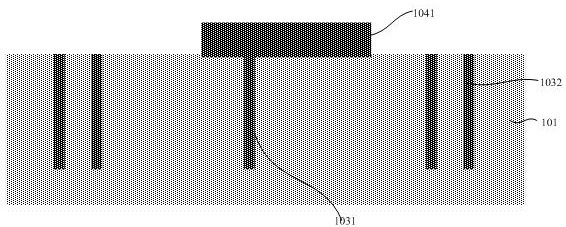
[0048] refer to Figure 8 , this embodiment provides a multilayer wiring adapter board, the multilayer wiring adapter board includes:

[0049] A substrate 101, wherein the substrate 101 has a first TSV column 1031 and a second TSV column 1032, and the first TSV column 1031 and the second TSV column 1032 both penetrate the substrate 101;

[0050] The first rewiring structure 104, the first rewiring structure 104 is located on the first surface of the substrate 101, including a first rewiring area A1 and a second rewiring area B1, in the first rewiring area A1 There is a first RDL metal wiring 1041, and there is a second RDL metal wiring 1042 in the second redistribution area B1, and the first RDL metal wiring 1041 is electrically connected to the first end of the first TSV column 1031, and the The second RDL metal wiring 1042 is electrically connected to the first end of the second TSV column 1032, and the thickness of the first RDL metal wiring 1041 is greater than the thickn...

Embodiment 2

[0082] refer to Figure 12 , this embodiment also provides a multilayer wiring adapter board, the difference between the multilayer wiring adapter board and the multilayer wiring adapter board in Embodiment 1 is that the first RDL metal is formed in this embodiment The step of wiring follows the step of forming two RDL metal wirings.

[0083] Specifically, the multilayer wiring adapter board includes:

[0084] a base 201, wherein the base 201 has a first TSV column 2031 and a second TSV column 2032, and the first TSV column 2031 and the second TSV column 2032 both penetrate the base 201;

[0085] The first rewiring structure 204, the first rewiring structure 204 is located on the first surface of the substrate 201, including a first rewiring area A2 and a second rewiring area B2, in the first rewiring area A2 There is a first RDL metal wiring 2041, and there is a second RDL metal wiring 2042 in the second redistribution area B2, and the first RDL metal wiring 2041 is electri...

Embodiment 3

[0091] refer to Figure 16 , this embodiment also provides a multilayer wiring adapter board, the difference between the multilayer wiring adapter board and the multilayer wiring adapter board in Embodiment 1 is that the first RDL metal is formed in this embodiment The step of wiring follows the step of forming two RDL metal wirings.

[0092] Specifically, the multilayer wiring adapter board includes:

[0093] a base 301, wherein the base 301 has a first TSV column 3031 and a second TSV column 3032, and the first TSV column 3031 and the second TSV column 3032 both penetrate the base 301;

[0094] The first rewiring structure 304, the first rewiring structure 304 is located on the first surface of the substrate 301, including a first rewiring area A3 and a second rewiring area B3, in the first rewiring area A3 There is a first RDL metal wiring 3041, and there is a second RDL metal wiring 3042 in the second redistribution area B3, and the first RDL metal wiring 3041 is electri...


PUM

PropertyMeasurementUnit
thicknessaaaaaaaaaa
thicknessaaaaaaaaaa
thicknessaaaaaaaaaa

Abstract

The invention provides a multilayer wiring adapter plate and a preparation method thereof. A first rewiring structure electrically connected with TSV columns is prepared on a first surface of a substrate, a second rewiring structure electrically connected with the TSV columns is prepared on a second surface of the substrate, the first rewiring structure comprises a first rewiring area and a second rewiring area, a first RDL metal wire is arranged in the first rewiring area, a second RDL metal wire is arranged in the second rewiring area, and the thickness of the first RDL metal wire is larger than that of the second RDL metal wire. Through partitioning of the RDL metal wires with different thicknesses, transmission requirements of different current densities can be met so as to provide a proper transmission channel, meanwhile, the problems of preparation and stress of the adapter plate can be solved, subsequent surface mounting is facilitated, and the reliability of a device is improved.

Description

technical field [0001] The invention belongs to the technical field of semiconductors, and relates to a multilayer wiring transfer board and a preparation method thereof. Background technique [0002] The multi-layer wiring adapter board refers to the setting of multi-layer structure on the silicon base material by means of RDL metal wiring. The RDL metal layer and the RDL metal layer can be isolated by insulating layers such as PI or silicon oxide, and the RDL metal layer Wiring can be made by Damascus or electroplating. Among them, the multilayer wiring interposer was first made by the previous process, such as nano-scale copper Damascus process, and IMD (In-Mold Decoration) polishing process. The advantage of this is that it can make multi-layer on the substrate. wiring structure, and the substrate will not deform due to stress. [0003] Multi-layer wiring can solve the problem of signal interconnection and integration, but for the conduction of some large currents in t...

Claims


Application Information

Patent Timeline
Patent Type & Authority Applications(China)
IPC IPC(8): H01L23/498H01L23/528H01L21/48
CPCH01L21/4857H01L21/486H01L23/49805H01L23/49822H01L23/49827H01L23/49838H01L23/5283H01L2224/02317H01L2224/02331H01L2224/02372H01L2224/02373H01L2224/02381
Inventor 冯光建马飞黄雷郭西高群
Owner 浙江集迈科微电子有限公司
Learn More