
Mini LED backlight plate manufacturing method and Mini LED backlight plate

A manufacturing method and technology for backlight panels, which are used in semiconductor devices, electrical components, circuits, etc., can solve problems such as rising product costs, inability to form patterns on passivation coatings, and difficulty in reaching the surface of metal markers, reducing product costs. cost effect

Active Publication Date: 2021-06-29
TCL CHINA STAR OPTOELECTRONICS TECH CO LTD
View PDF6 Cites 2 Cited by
  • Summary
  • Abstract
  • Description
  • Claims
  • Application Information

AI Technical Summary

Problems solved by technology

An existing passivation coating is formed by coating the surface of the substrate with a passivation coating. For passivation coating materials with high reflectivity, most of the light from the light source is directly reflected after passing through the passivation coating. out, but it is difficult to reach the surface of the metal marker, and it is impossible to accurately align the exposure machine, resulting in the failure of the passivation coating to form the set pattern; in addition, when the passivation coating process is completed and then cut into the corresponding size, Due to the high film thickness of the passivation coating and the inherent characteristics of the material, the passivation coating in the cutting area tends to be jagged during cutting, and in severe cases, it will cause edge cracks and fall off
Another existing form of passivation coating is that no passivation coating is applied on the entire edge of the metal marker on the surface of the substrate, so that the CCD lens can read the position of the metal marker to accurately align the exposure machine. Positioning, but the edge area of ​​the substrate is wasted, and the maximum utilization of the substrate cannot be achieved, which will lead to a sharp increase in product costs

Method used


Image

  • Mini LED backlight plate manufacturing method and Mini LED backlight plate
  • Mini LED backlight plate manufacturing method and Mini LED backlight plate
  • Mini LED backlight plate manufacturing method and Mini LED backlight plate

Examples


Embodiment Construction

[0050] The technical solutions in the embodiments of the present application will be clearly and completely described below in conjunction with the drawings in the embodiments of the present application. Apparently, the described embodiments are only some of the embodiments of this application, not all of them. Based on the embodiments in this application, all other embodiments obtained by those skilled in the art without making creative efforts belong to the scope of protection of this application.

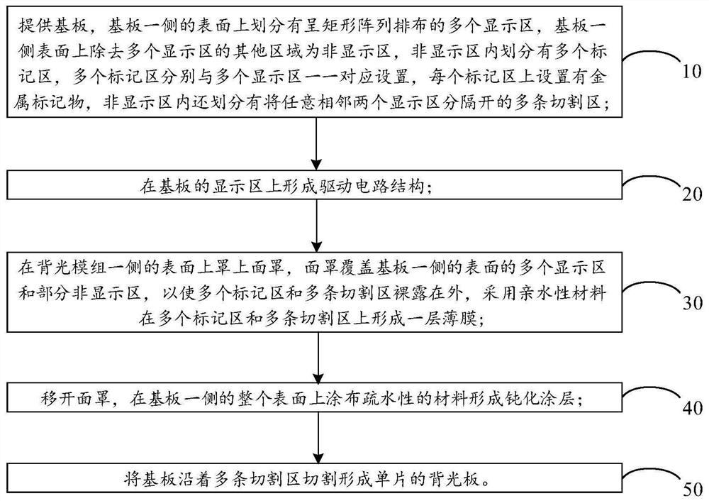
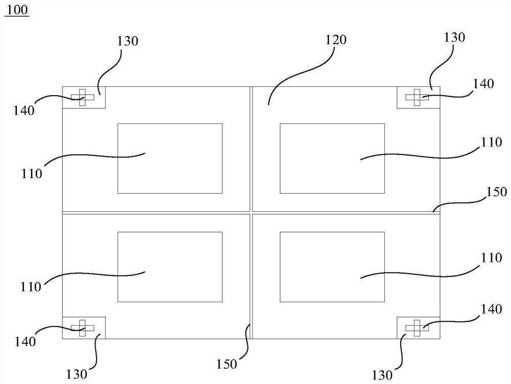
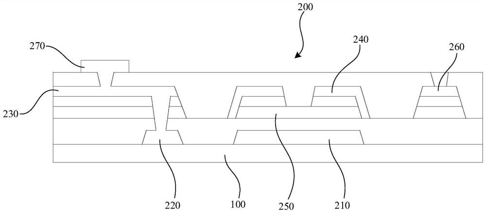
[0051] see Figure 1-14 , figure 1 A block flow diagram of a manufacturing method of a Mini LED backlight panel provided by the embodiment of the present application, figure 2 The first process flow diagram provided by the embodiment of the present application, image 3 Schematic diagram of the structure of the Mini LED backlight panel provided in the embodiment of this application, Figure 4 A flow chart of forming a driving circuit structure provided by the embodiment of t...


PUM

PropertyMeasurementUnit
thicknessaaaaaaaaaa

Abstract

An embodiment of the invention provides a Mini LED backlight plate manufacturing method and a Mini LED backlight plate. The Mini LED backlight plate manufacturing method comprises the following steps of: providing a substrate, dividing at least one display region on the substrate, dividing at least one mark region in a non-display region, and arranging metal markers on the mark regions; covering the substrate with a mask, exposing the at least one marking region outside, and forming a layer of film on the at least one marking region by adopting a hydrophilic material; and removing the mask, and coating a hydrophobic passivation coating on the whole surface of the substrate. According to the manufacturing method disclosed by the embodiment of the invention, a hydrophilic thin film formed on the at least one mark region can enable the hydrophobic passivation coating to be difficult to form a film during coating and expose the metal markers, so that an exposure machine can be accurately positioned, and a passivation coating with a set pattern can be formed; meanwhile, other regions of the substrate can be coated with passivation coatings, the maximum utilization rate of the substrate can be achieved, and the product cost is reduced.

Description

technical field [0001] The present application relates to the field of display technology, in particular to a method for manufacturing a Mini LED backlight panel and the Mini LED backlight panel. Background technique [0002] In order to ensure the stability of thin film transistor devices in the production of Mini LED backlights, and to maximize light utilization and optical quality, there is a passivation coating process, the thickness of the passivation coating is <30um, and the reflectivity is >80%. . In order to enable the passivation coating to form a pattern at the set position, it is necessary to set a metal marker on the surface of the substrate for alignment of the exposure machine. When the exposure machine uses the set metal marker for alignment, the light source penetrates the passivation The coating is reflected on the metal marker, and then input into the CCD (charge-coupled device) lens with the function of detecting reflected light, so as to complete ...

Claims


Application Information

Patent Timeline
Patent Type & Authority Applications(China)
IPC IPC(8): H01L27/15H01L33/44
CPCH01L27/156H01L33/44H01L2933/0025H01L25/167H01L25/0753H01L27/1248H01L27/1288
Inventor 李兰艳
Owner TCL CHINA STAR OPTOELECTRONICS TECH CO LTD
Learn More