Transparent perfect microwave absorber based on graphene/transparent medium and ultrathin doped metal

A transparent medium, graphene technology, applied in the fields of magnetic/electric field shielding, electrical components, etc., can solve the problem of lack of high-performance broadband microwave absorption technology, inability to completely eliminate electromagnetic interference, etc., to achieve high-performance transparent perfect electromagnetic absorption, broadening Electromagnetic absorption frequency band, realizing the effect of electromagnetic absorption

Pending Publication Date: 2021-06-29
HARBIN INST OF TECH
View PDF15 Cites 1 Cited by
  • Summary
  • Abstract
  • Description
  • Claims
  • Application Information

AI Technical Summary

Problems solved by technology

[0021] The purpose of the present invention is to overcome the deficiencies of the above-mentioned existing transparent electromagnetic shielding technology, especially for metal-based conductive transparent electromagnetic shielding technology that mainly causes secondary electromagnetic pollution due to electromagnetic reflection, cannot completely eliminate electromagnetic interference and lacks high-performance broadband microwave The problem of absorption technology is to develop a transparent microwave absorbing device based on multi-layer graphene / transparent medium and ultra-thin doped metal composite resonant cavity, using ultra-thin doped metal as a transparent electromagnetic reflection structure to achieve strong electromagnetic reflection in a wide frequency band At the same time, multiple Fabry-Perot resonators are constructed by using multi-layer graphene / transparent medium combination units, which can absorb multiple frequency points with high performance and broaden the electromagnetic absorption frequency band

Method used


Image

  • Transparent perfect microwave absorber based on graphene/transparent medium and ultrathin doped metal
  • Transparent perfect microwave absorber based on graphene/transparent medium and ultrathin doped metal
  • Transparent perfect microwave absorber based on graphene/transparent medium and ultrathin doped metal

Examples


Embodiment Construction

[0043] Embodiment of the present invention is described in detail below in conjunction with accompanying drawing:

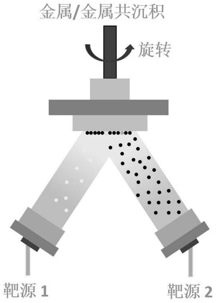
[0044] attached figure 1 It is a schematic diagram of the preparation of an ultra-thin doped metal film based on a metal / metal co-doped deposition process according to the present invention. A high-purity silver target or copper target or gold target is used as a target source for deposition (target source 2), and the other target source (target source 1) is a deposition source for doped metals (aluminum, titanium, nickel, chromium, tantalum, germanium). It should be noted that when preparing the doped silver film, the doping metal of the target source 1 can be selected as copper. By changing the power of the two target power sources, the deposition speeds of the two can be adjusted, thereby changing the ratio of the deposited atomic concentrations of the two in the doped metal film.

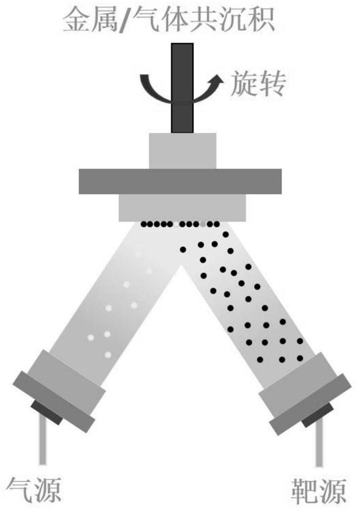
[0045] attached figure 2 It is a schematic diagram of the preparation of a...


PUM

PropertyMeasurementUnit
Thicknessaaaaaaaaaa

Abstract

The invention discloses a transparent perfect microwave absorber based on a graphene / transparent medium and ultrathin doped metal, and belongs to the field of optical transparent part electromagnetic shielding. According to the transparent perfect microwave absorber, a high-quality doped metal film with a continuous surface and extremely low roughness is obtained under the ultra-thin thickness condition by utilizing a co-doping deposition method. Graphene and a transparent medium form a graphene / transparent medium unit, and then the graphene / transparent medium unit and ultrathin doped metal form a microwave resonant cavity. The thickness of the ultrathin doped metal film is less than dozens of nanometers and is far less than the wavelength of microwave band electromagnetic waves, so that stable wide-band strong electromagnetic reflection can be provided, the problem that the electromagnetic reflectivity of a reflecting layer in a traditional microwave resonant cavity has frequency dependence is solved, and a novel electromagnetic reflection structure is provided for a microwave absorber. Furthermore, the thickness of the corresponding transparent dielectric layer is obtained through theoretical modeling analysis, perfect absorption of microwaves at designed frequency points can be achieved, a multi-frequency-point resonant cavity can be formed by using the multilayer graphene / transparent dielectric unit and the ultrathin doped metal, absorption resonance of multiple frequency points is introduced, the absorption bandwidth of the microwave absorber is greatly expanded, and high-performance broadband microwave absorption is realized.

Description

technical field [0001] The invention belongs to the field of electromagnetic shielding of optical transparent parts, in particular to a transparent perfect microwave absorber based on graphene / transparent medium and ultra-thin doped metal. Background technique [0002] From radio, television, radar, satellite communication and navigation, mobile communication to wireless positioning, medical diagnosis, etc., electromagnetic wave technology is widely used in various fields of people's daily life and production. Especially with the continuous development of electromagnetic wave communication technology, the terminal equipment for transmitting and receiving electromagnetic waves has increased by an order of magnitude, the electromagnetic wave application band has been continuously broadened, and the electromagnetic wave transmission power has been continuously enhanced, resulting in increasingly serious electromagnetic pollution problems. One of its effects is that the broadeni...

Claims


Application Information

Patent Timeline
IPC IPC(8): H05K9/00
CPCH05K9/0088
Inventor 王赫岩陆振刚谭久彬
Owner HARBIN INST OF TECH
Why Eureka
Try Eureka