Light source plate and preparation method thereof and display device
A light source board and substrate technology, which is applied in the direction of instruments, optics, semiconductor devices, etc., can solve the problems of cumbersome Mini-LED chip technology, etc., and achieve the effect of improving welding yield, improving positioning accuracy, and high welding strength
- Summary
- Abstract
- Description
- Claims
- Application Information
AI Technical Summary
Problems solved by technology
Method used
Image

Examples
preparation example Construction
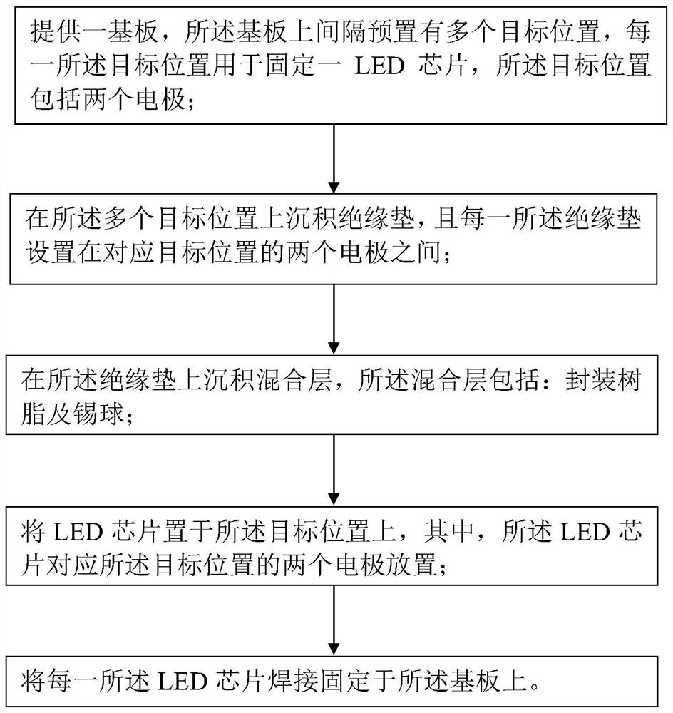
[0033] A preparation method of a light source plate, such as figure 1 shown, including the following steps:
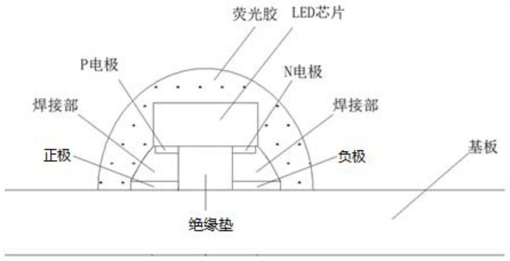
[0034] S01. Provide a substrate, on which a plurality of target positions are preset at intervals, each of the target positions is used to fix an LED chip, and the target positions include two electrodes;
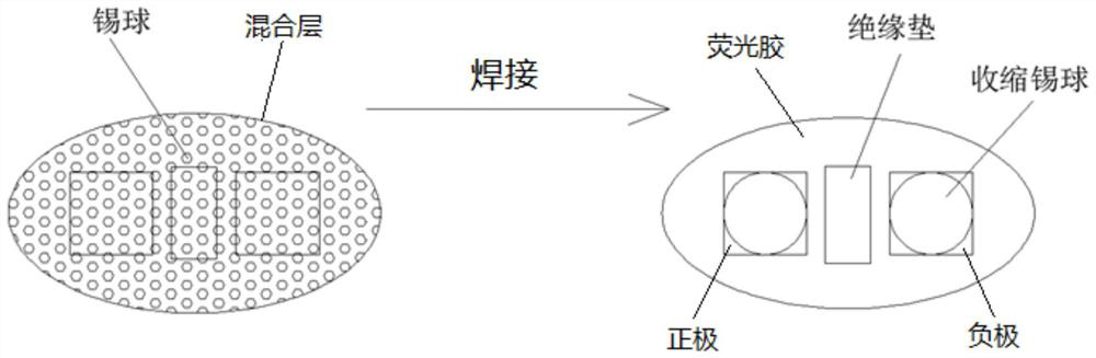
[0035] S02. Deposit insulating pads on the plurality of target positions, and each of the insulating pads is disposed between two electrodes corresponding to the target positions;
[0036] S03. Deposit a mixed layer on the insulating pad, where the mixed layer includes: packaging resin and solder balls;
[0037] S04. Place the LED chip on the target position, wherein the LED chip is placed corresponding to the two electrodes of the target target position;
[0038] S05. Solder and fix each of the LED chips on the substrate.
[0039] The preparation method of the light source board provided by the embodiment of the present invention is to deposit insulating pads on...
Embodiment approach
[0063] As an implementation manner, the mixed layer further includes: fluorescent powder;
[0064] Wherein, the weight percentage of the fluorescent powder is 10%-30%, the weight percentage of the packaging resin is 10%-50%, and the weight percentage of the solder ball is 30%-60%;
[0065] Phosphor powder is added to the mixed layer. On the one hand, the phosphor powder is lighter than the tin ball, so that the phosphor powder in the mixture can be cured with the packaging resin to form a fluorescent glue that wraps the LED chip; on the other hand, the phosphor powder can convert the light emitted by the chip. Color, by using this feature to achieve flexible adjustment of the light color of the light source board, the flexible adjustment of the light color of the backlight can be realized in the absence of quantum dot films, reducing the use of expensive quantum dot materials, and at the same time, in the preparation of RGB For the three-color backlight, only LED chips with lo...
Embodiment 1
[0121] In this embodiment, a monochromatic light source board is prepared, which specifically includes the following steps:
[0122] (1) Deposit insulating pads on the substrate
[0123] A substrate is provided, and a plurality of target positions are preset at intervals on the substrate, and each target position is used to fix an LED chip, and the target positions include positive poles and negative poles;
[0124] Preset a stencil, such as Figure 5 As shown, the stencil is provided with a plurality of through holes, and each through hole is arranged between the positive electrode and the negative electrode corresponding to the target position; the stencil is placed on the substrate, and each of the through holes corresponds to a target position ;
[0125] A thixotropic silica gel layer is coated on the steel mesh, so that the thixotropic silica gel is printed on the substrate through the through hole to form a thixotropic silica gel layer; the steel mesh is removed, and t...
PUM
| Property | Measurement | Unit |
|---|---|---|
| Viscosity | aaaaa | aaaaa |
| Width | aaaaa | aaaaa |
| Length | aaaaa | aaaaa |
Abstract
Description
Claims
Application Information
 - R&D
- Intellectual Property
- Life Sciences
- Materials
- Tech Scout
- Unparalleled Data Quality
- Higher Quality Content
- 60% Fewer Hallucinations
Browse by: Latest US Patents, China's latest patents, Technical Efficacy Thesaurus, Application Domain, Technology Topic, Popular Technical Reports.
© 2025 PatSnap. All rights reserved.Legal|Privacy policy|Modern Slavery Act Transparency Statement|Sitemap|About US| Contact US: help@patsnap.com