
A high-voltage and fast silicon carbide diode and its preparation method

A technology of silicon carbide diodes and silicon carbide, which is applied in semiconductor/solid-state device manufacturing, semiconductor devices, electrical components, etc., can solve the problems of low voltage, slow conduction speed, and small Schottky barrier area of ​​silicon carbide diodes, etc. Achieve the effects of fast conduction speed, large voltage and large area

Active Publication Date: 2021-11-12
先之科半导体科技(东莞)有限公司
View PDF10 Cites 0 Cited by
  • Summary
  • Abstract
  • Description
  • Claims
  • Application Information

AI Technical Summary

Problems solved by technology

[0003] Traditional silicon carbide diodes usually set the silicon dioxide layer at N - The upper end of the silicon carbide epitaxial layer, and then the anode metal is deposited on the inner side of the silicon dioxide layer, resulting in anode metal and N - The area of ​​the Schottky barrier formed between the silicon carbide epitaxial layers is small, so that the forward conduction voltage of the silicon carbide diode is low, and the conduction speed is slow. For some high-voltage and fast circuits, the conditions cannot be met.

Method used


Image

  • A high-voltage and fast silicon carbide diode and its preparation method
  • A high-voltage and fast silicon carbide diode and its preparation method
  • A high-voltage and fast silicon carbide diode and its preparation method

Examples


Embodiment 1

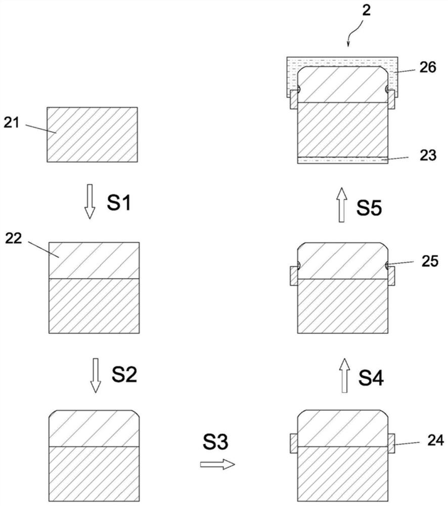
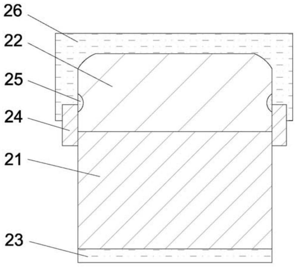
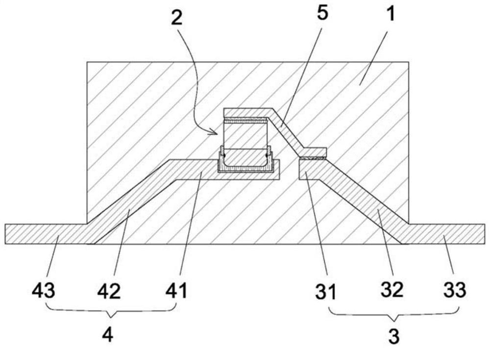
[0029] like Figure 1-3 Shown:

[0030] A high-voltage and fast silicon carbide diode, including a silicon carbide diode, the silicon carbide diode includes a plastic package 1, a silicon carbide chip 2, a cathode pin 3, an anode pin 4, and a welding aid 5, and the silicon carbide chip 2 includes N + SiC substrate 21, covered in N + N on the upper end of the silicon carbide substrate 21 - SiC epitaxial layer 22, covered in N + The cathode metal 23 at the lower end of the silicon carbide substrate 21 is located at N + SiC substrate 21 with N - The silicon dioxide layer 24 on the outer side of the junction of the silicon carbide epitaxial layer 22 is located at N + SiC substrate 21 with N - The P-type guard ring 25 inside the junction of the silicon carbide epitaxial layer 22 covers the silicon dioxide layer 24, N - The anode metal 26 on the upper end of the silicon carbide epitaxial layer 22, the anode metal 26 is welded to the anode pin 4, one end of the welding aid pla...


PUM


Abstract

The invention provides a high-voltage and fast silicon carbide diode and a preparation method thereof, including a silicon carbide diode, the silicon carbide diode including a plastic package, a silicon carbide chip, a cathode pin, an anode pin, and a soldering aid plate. Silicon chips include N + SiC substrate, N ‑ SiC epitaxial layer, cathode metal, silicon dioxide layer, P-type guard ring, covering the silicon dioxide layer, N ‑ An anode metal on the upper end of the silicon carbide epitaxial layer, the anode metal is welded to the anode pin, one end of the welding aid plate is welded to the cathode pin, and the other end is welded to the cathode metal. Silicon carbide diode of the present invention and preparation method thereof, silicon dioxide layer is grown on N + SiC substrate with N ‑ The outer side of the silicon carbide epitaxial layer junction, on the silicon dioxide layer, N ‑ A layer of anode metal is deposited on the upper end of the silicon carbide epitaxial layer. In the formed structure, the Schottky barrier area is large, the voltage that can pass through the silicon carbide diode in the forward direction is large, and the conduction speed is fast.

Description

technical field [0001] The invention relates to the technical field of Schottky rectifiers, in particular to a high-voltage and fast silicon carbide diode and a preparation method thereof. Background technique [0002] Silicon carbide materials have the characteristics of wide band gap, high breakdown field strength, high thermal conductivity, high saturation electron mobility and excellent physical and chemical stability, and are suitable for working in high temperature, high frequency, high power and extreme environments, so Some diodes are made of silicon carbide diodes using silicon carbide materials instead of traditional silicon materials. [0003] Traditional silicon carbide diodes usually set the silicon dioxide layer at N - The upper end of the silicon carbide epitaxial layer, and then the anode metal is deposited on the inner side of the silicon dioxide layer, resulting in anode metal and N - The area of ​​the Schottky barrier formed between the silicon carbide e...

Claims


Application Information

Patent Timeline
Patent Type & Authority Patents(China)
IPC IPC(8): H01L29/06H01L29/872H01L21/329
CPCH01L29/0649H01L29/0661H01L29/6606H01L29/872
Inventor 刘柏光
Owner 先之科半导体科技(东莞)有限公司
Learn More