Printed circuit board (PCB) manufacturing process

A printed circuit board and manufacturing process technology, applied in the direction of printed circuit manufacturing, printed circuit, printed circuit drying, etc., can solve the problems of PCB unit board surface pollution, out-of-tolerance expansion and shrinkage, scrap, etc., to avoid pollution, The effect of increasing the glass transition temperature

Active Publication Date: 2021-07-20
GUANGZHOU MEADVILLE ELECTRONICS
View PDF6 Cites 0 Cited by
  • Summary
  • Abstract
  • Description
  • Claims
  • Application Information

AI Technical Summary

Problems solved by technology

However, due to the influence of high temperature and high pressure on the solder resist ink on the PCB unit board, the solder resist ink on the adjacent PCB unit board is prone to adhesion during the direct return process, resulting in copper-exposed defects on the PCB unit board.
However, if white paper is used to separate adjacent PCB unit boards, the PCB unit boards will have problems such as surface pollution and out-of-tolerance expansion and shrinkage, which will eventually lead to scrapping

Method used


Image

  • Printed circuit board (PCB) manufacturing process
  • Printed circuit board (PCB) manufacturing process
  • Printed circuit board (PCB) manufacturing process

Examples


Embodiment Construction

[0027] Below, the present invention will be further described in conjunction with the accompanying drawings and specific implementation methods. It should be noted that, under the premise of not conflicting, the various embodiments described below or the technical features can be combined arbitrarily to form new embodiments. .

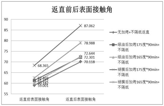
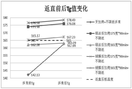
[0028] Such as Figure 1-7 As shown, in the production process of PCB printed circuit boards, in order to ensure that the expansion and shrinkage of the finished board can meet the tolerance required by customers (generally control ±3mil), after the PCB substrate is divided into PCB unit boards, a return straight baking board will be added The process releases the thermal stress in the board, so as to be able to straighten the PCB unit board, etc. where the board is bent and warped, so as to ensure that the size of the finished board meets the customer's requirements. The production process of the existing PCB printed circuit board is as follows: sold...


PUM


Abstract

The invention discloses a PCB manufacturing process, which comprises a solder mask manufacturing step, a electroless nickel immersion gold (ENIG) step, a baking step, a dividing step and a straightening step, and can avoid the defect of copper exposure on PCB unit boards caused by bonding of solder resist ink on adjacent PCB unit boards in a straightening process. And meanwhile, the plate surface pollution and the expansion and shrinkage size out-of-tolerance are avoided.

Description

technical field [0001] The invention relates to the technical field of PCB board manufacturing, in particular to a PCB printed circuit board manufacturing process. Background technique [0002] In the PCB printed circuit board, in order to ensure that the expansion and shrinkage of the finished board can meet the tolerance required by the customer (generally control ±3mil), after the PCB substrate is divided into PCB unit boards, the process of returning to the straight baking board will be added, and the board will be directly baked. Release the thermal stress inside, so as to be able to straighten the PCB unit board, etc. where the board is bent and warped, so as to ensure that the size of the finished board meets the customer's requirements. However, due to the impact of high temperature and high pressure on the solder resist ink on the PCB unit board, the solder resist ink on the adjacent PCB unit board is prone to adhesion during the direct return process, resulting in ...

Claims


Application Information

Patent Timeline
Patent Type & Authority Applications(China)
IPC IPC(8): H05K3/22H05K3/18H05K3/28
CPCH05K3/227H05K3/18H05K3/225H05K3/282
Inventor 何锦添彭浪祥许杏芳彭智新
Owner GUANGZHOU MEADVILLE ELECTRONICS
Why Eureka
Try Eureka