Pinhole high-definition imaging device and pinhole imaging system

An imaging device and pinhole imaging technology, applied in the field of pinhole imaging, can solve the problems of recorded information distortion, destruction of incident light spectrum information, etc., and achieve the effects of weakening light intensity, reducing diffraction efficiency, and high imaging resolution

Active Publication Date: 2021-07-30
LASER FUSION RES CENT CHINA ACAD OF ENG PHYSICS
View PDF15 Cites 0 Cited by
  • Summary
  • Abstract
  • Description
  • Claims
  • Application Information

AI Technical Summary

Problems solved by technology

[0004] When the x-ray energy is very strong, in order to protect the imaging equipment from being damaged, it is usually necessary to add a metal filter in...

Method used


Image

  • Pinhole high-definition imaging device and pinhole imaging system
  • Pinhole high-definition imaging device and pinhole imaging system
  • Pinhole high-definition imaging device and pinhole imaging system

Examples


Embodiment Construction

[0021] The present invention will be further described below in conjunction with embodiment and accompanying drawing.

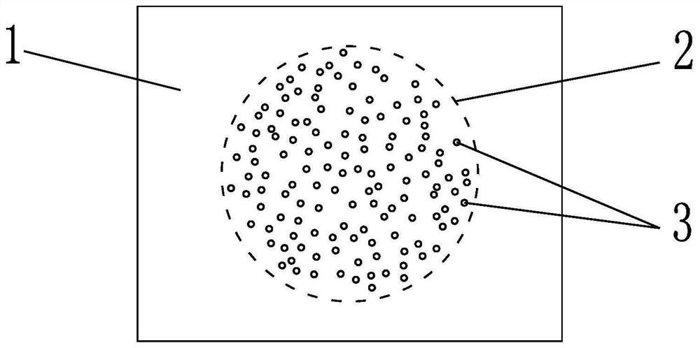
[0022] Such as figure 1 The pinhole high-definition imaging device shown is used in the field of pinhole imaging. For the convenience of description, the imaging device is referred to as a "pinhole screen" hereinafter.

[0023] The pinhole sieve includes a substrate 1 of metal or non-metallic material that is set to be opaque as required. There is a circular pinhole area 2 on the substrate 1. The diameter of the pinhole area 2 is on the order of ten microns, that is, 10~ In the interval of 100 microns, there are a large number of micro-nano holes 3 distributed in the pinhole area 2, and the pore diameters of the micro-nano holes 3 are basically the same, the range is on the order of hundreds of nanometers, and the number is preferably 1000-10000 to basically cover the pinholes area 2.

[0024] The micro-nano holes 3 adopt a quasi-random distribution in the ...


PUM

PropertyMeasurementUnit
Diameteraaaaaaaaaa

Abstract

The invention discloses a pinhole high-definition imaging device which comprises a substrate with a pinhole area, the diameter of the pinhole area is 10-100 micrometers, micro-nano small holes distributed in an asymmetric mode are formed in the pinhole area, and the aperture of the micro-nano small holes is in the hundred-nanometer magnitude. The large number of micro-nano small holes are randomly distributed in the pinhole, so that diffraction of the pinhole can be inhibited, and the final imaging resolution of the pinhole is approximate to the description of geometrical optics within a certain limit. Compared with pinhole imaging with the same aperture, the device breaks through the limitation of diffraction on the aperture of the pinhole, the pinhole can be made smaller, and the final imaging resolution is higher. Compared with performance of traditional pinhole imaging, the diffraction efficiency of a system is reduced through the large number of micro-nano small holes, the effect of a neutral filter is achieved, and the light intensity of incident light can be weakened on the premise that spectral information of the incident light is not changed so that imaging equipment can be protected. The invention further discloses a pinhole imaging system with the pinhole high-definition imaging device.

Description

technical field [0001] The invention relates to the technical field of pinhole imaging, in particular to a pinhole high-definition imaging device and a pinhole imaging system. Background technique [0002] Inertial confinement fusion is expected to become an effective way to cleanly utilize fusion energy in the future. It has important research value in the fields of people's livelihood, economy and military. The United States, China, Russia and other major countries have carried out a series of in-depth researches on laser inertial confinement fusion. [0003] In the research of laser inertial confinement fusion, in order to study the physical phenomena in the experiment, pinhole imaging is a commonly used X-ray imaging method. The pinhole camera and framing camera based on the principle of pinhole imaging are widely used in laser fusion research. Therefore, it is of great significance to improve the resolution of pinhole imaging. [0004] When the X-ray energy is very str...

Claims


Application Information

Patent Timeline
IPC IPC(8): G03B42/02G02B27/58
CPCG03B42/021G02B27/58
Inventor 王峰刘欣城理玉龙徐涛刘祥明魏惠月彭晓世关赞洋刘永刚任宽杨冬杨家敏江少恩何海恩
Owner LASER FUSION RES CENT CHINA ACAD OF ENG PHYSICS
Why Eureka
Try Eureka