High-transmittance atomic beam microscopic apparatus

A high-transmittance, atomic-beam technology, applied in measurement devices, material analysis using wave/particle radiation, instruments, etc., can solve the problems of insufficient focusing of atomic beams, limited atomic transmittance, and difficult processing, etc., to achieve Sharp focus beam spot, suppress diffraction, optimize focus effect

Pending Publication Date: 2018-12-07
JINHUA VOCATIONAL TECH COLLEGE
View PDF11 Cites 0 Cited by
  • Summary
  • Abstract
  • Description
  • Claims
  • Application Information

AI Technical Summary

Problems solved by technology

[0003] The defect of the existing technology is that in a working mode of the atomic beam microscope, the Fresnel zone plate is used to focus the atoms in the form of de Broglie matter waves, and the ultimate resolution is determined by the outermost part of the Fresnel zone. Due to the low energy of the atomic beam, the atoms will not penetrate the solid material, so the ring used to transmit the atoms on the Fresnel zone plate must adopt an unsupported structure, which is relatively difficult in processing. In addition, the through-holes of some atomic diffraction sheets with a through-hole structure are randomly distributed, and the disadvantage is that the number of through-holes on a certain cross-sectional area of ​​the atomic beam is limited, the atomic transmittance is limited, and the atomic beam The focusing effect is not good enough, and the beam spot will be interfered by high-order diffraction. The high-transmittance atomic beam microscopic device can solve the problem

Method used


Image

  • High-transmittance atomic beam microscopic apparatus
  • High-transmittance atomic beam microscopic apparatus
  • High-transmittance atomic beam microscopic apparatus

Examples


Embodiment Construction

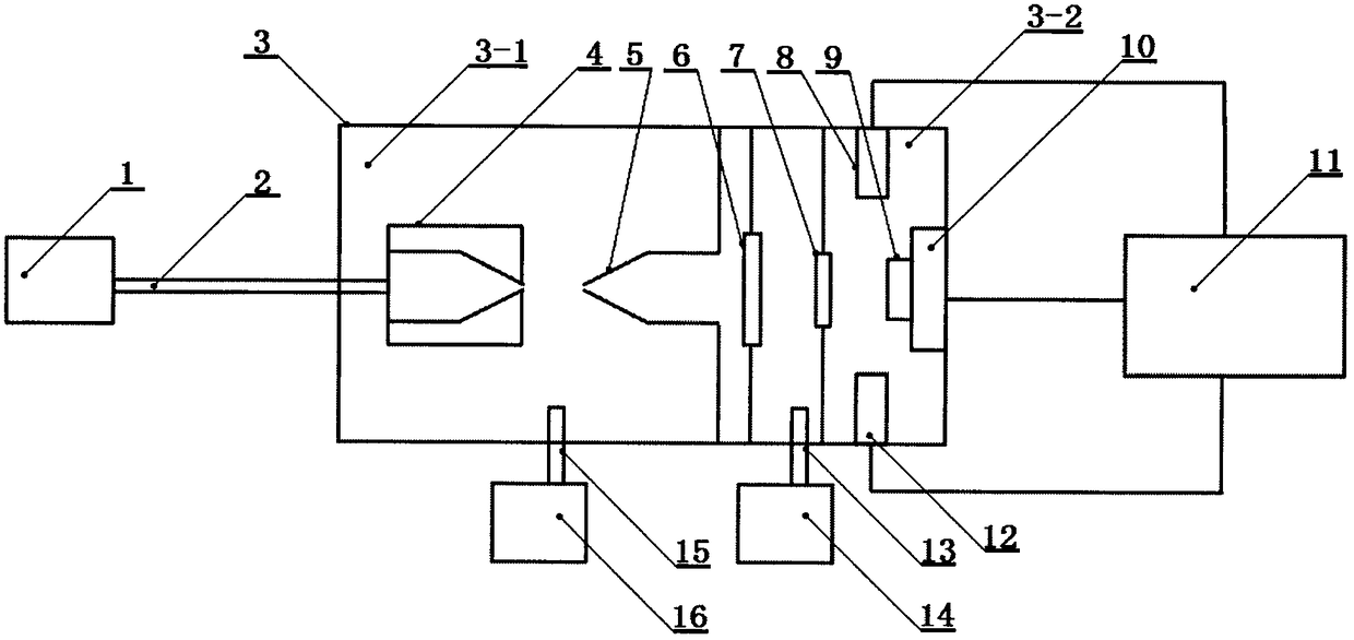
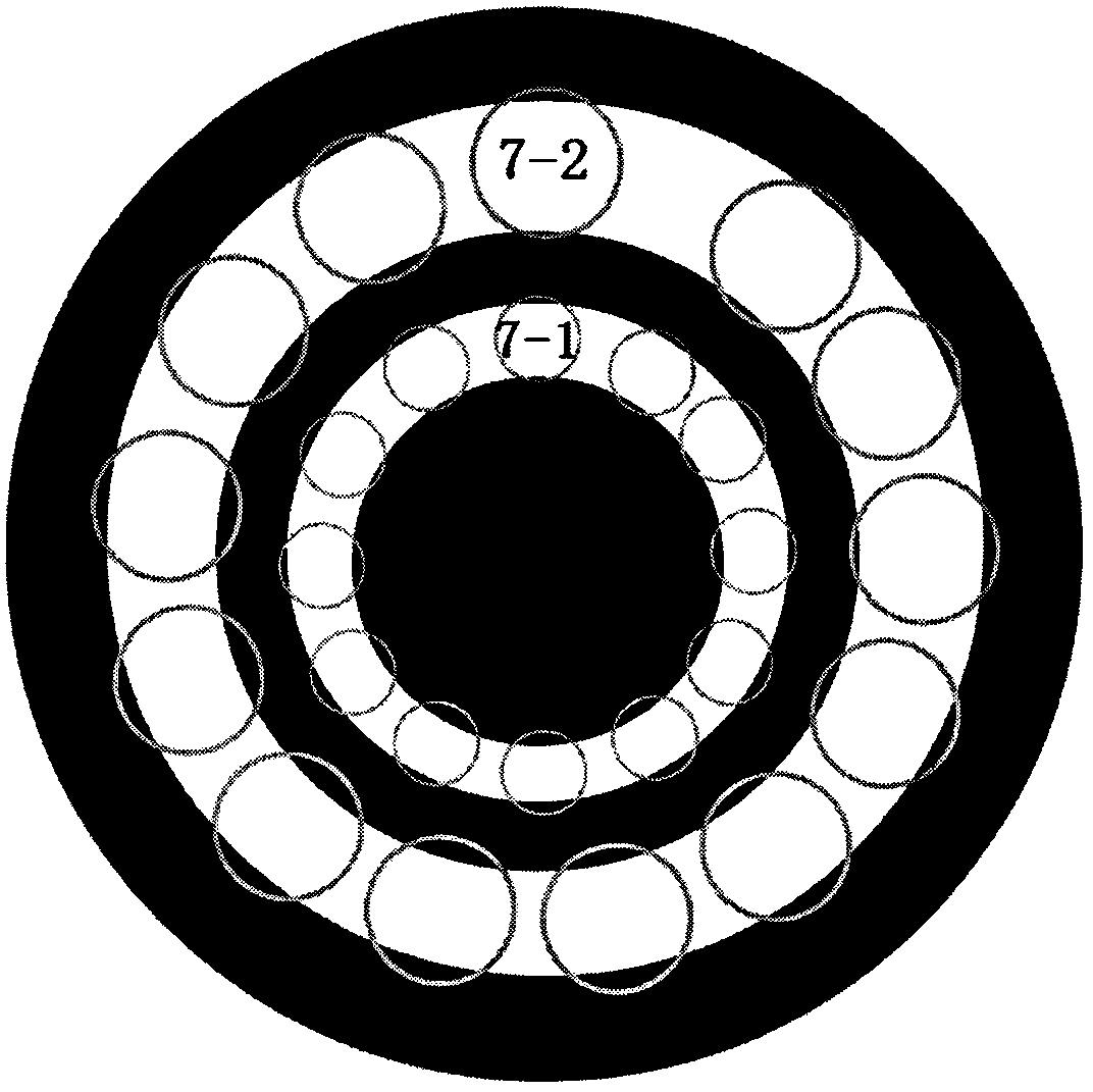
[0026] Such as figure 1It is a schematic diagram of the present invention, mainly comprising a gas storage tank (1), a gas pipe (2), a vacuum chamber (3) connected by a chamber body I (3-1) and a chamber body II (3-2), and a spray head ( 4), splitter (5), gas transmission window (6), atomic diffraction sheet (7), through hole (7-1) on the transmission area of ​​the first-order Fresnel ring zone, second-order Fresnel Through hole (7-2) on the transmission area of ​​the annular zone, detector I (8), sample (9), sample stage (10), computer (11), detector II (12), gas extraction port I (13) , vacuum pump group I (14), air inlet II (15), vacuum pump group II (16), the cavity I (3-1) and cavity II (3-2) are connected by a flow divider (5), and the cavity The body II (3-2) is connected to the vacuum pump group I (14) through the suction port I (13), the cavity I (3-1) is connected to the vacuum pump group II (16) through the suction port II (15), and the detector I (8 ) is the same...


PUM

PropertyMeasurementUnit
diameteraaaaaaaaaa
thicknessaaaaaaaaaa
thicknessaaaaaaaaaa

Abstract

The invention relates to the technical field of microscopy of materials and provides a high-transmittance atomic beam microscopic apparatus including a gas tank, a gas pipe, a vacuum chamber formed byconnecting a first chamber and a second chamber, a jet head, a splitter, a gas transmittance window slice, an atom diffraction slice, through holes in a first-stage Fresnel zone plate transmission area, through holes in a second-stage Fresnel zone plate transmission area, a first detector, a sample, a sample table, a computer, a second detector, a first gas suction port, a first vacuum pump set,a second gas suction port and a second vacuum pump set. The first detector and the second detector respectively detect the atoms that are reflected by the surface of the sample and work under a differential pair mode. The atom diffraction slice with through holes is easy to manufacture, wherein the through holes are orderly arranged according to corresponding Fresnel zones, so that the total areaof through holes in the cross section are of a certain atomic beam flow can be increased, and the transmittance of the atomic beam flow is increased. The apparatus can form a sharp focusing beam spotand inhibit higher-order diffraction, thereby increasing the signal-to-noise ratio of the apparatus.

Description

technical field [0001] The invention relates to the field of microscopic technology for materials, in particular to a high-transmittance atomic beam microscopic device with a specially designed atomic diffraction sheet. Background technique [0002] In the field of microscopic technology, the existing electron microscope can only image conductive samples, and the electron beam emitted by the electron microscope is of high energy, which will cause some sensitive sample surfaces to be damaged by radiation. The atomic beam microscope can overcome the above defects and image fragile or insulating samples. It usually uses inert gas atoms as the emitting atoms. The energy of the atomic beam of the inert gas is very low and its chemical properties are very stable. Obtain an image of the surface of the sample. The working principle of the atomic beam microscope is: in a high vacuum, the free atomic flow passes through the nozzle and the aperture to form a beam of gas atoms and shoo...

Claims


Application Information

Patent Timeline
Patent Type & Authority Applications(China)
IPC IPC(8): G01N23/20008
CPCG01N23/20008G01N2223/105G01N2223/05
Inventor 张向平赵永建
Owner JINHUA VOCATIONAL TECH COLLEGE
Why Eureka
Try Eureka