Semiconductor structure with micro-channel, chip stacking structure and preparation method

A chip stacking and semiconductor technology, which is applied in semiconductor devices, semiconductor/solid-state device parts, electric solid-state devices, etc., can solve the problems of high difficulty and complexity in preparation, reduce the difficulty and complexity of preparation, and simplify the preparation method. Effect of Surface Cleanliness and Planarity Requirements

Active Publication Date: 2021-08-10
NAT CENT FOR ADVANCED PACKAGING
View PDF2 Cites 3 Cited by
  • Summary
  • Abstract
  • Description
  • Claims
  • Application Information

AI Technical Summary

Problems solved by technology

[0004] Therefore, the technical problem to be solved by the present invention is to overcome the defects of high difficulty and complexity in the preparation method of the existing microchannel structure, thereby providing a semiconductor structure with a microchannel, a chip stack structure and a preparation method

Method used


Image

  • Semiconductor structure with micro-channel, chip stacking structure and preparation method
  • Semiconductor structure with micro-channel, chip stacking structure and preparation method
  • Semiconductor structure with micro-channel, chip stacking structure and preparation method

Examples


Embodiment 1

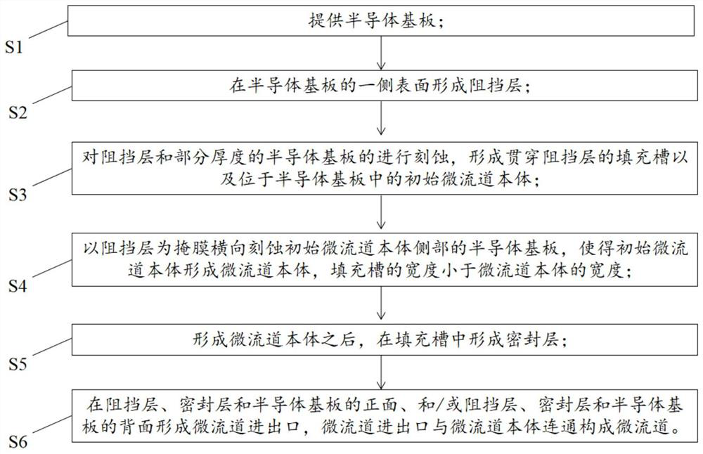
[0050] see figure 1 , the present embodiment provides a method for preparing a semiconductor structure with a microchannel, comprising the following steps:

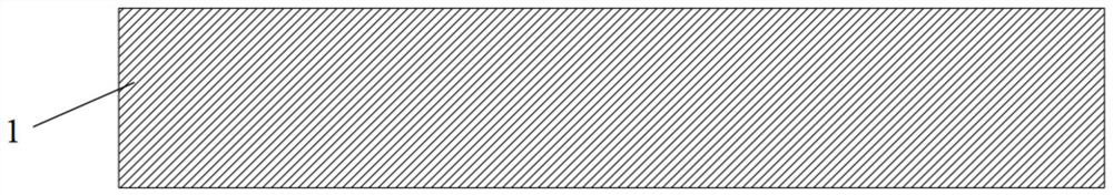
[0051] S1. Provide semiconductor substrates;

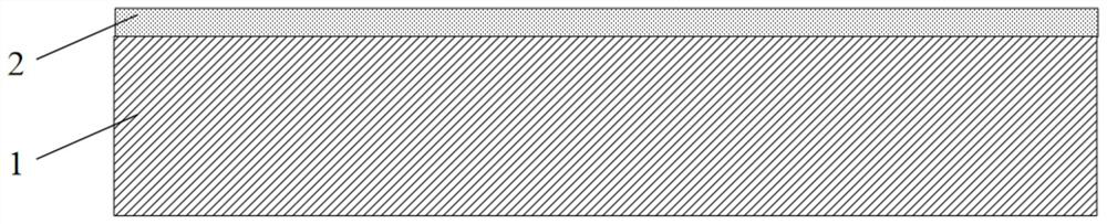
[0052] S2, forming a barrier layer on one side surface of the semiconductor substrate;

[0053] S3. Etching the barrier layer and part of the thickness of the semiconductor substrate to form a filling groove penetrating through the barrier layer and an initial microchannel body located in the semiconductor substrate;

[0054] S4, using the barrier layer as a mask to laterally etch the semiconductor substrate on the side of the initial microchannel body, so that the initial microchannel body forms a microchannel body, and the width of the filling groove is smaller than that of the microchannel the width of the body;

[0055] S5, after forming the micro-channel body, forming a sealing layer in the filling groove;

[0056] S6, forming a micro-channel inlet and outlet on the ...

Embodiment 2

[0088] This embodiment provides a method for preparing a stacked chip structure, including: forming a semiconductor structure. The method for forming the semiconductor structure adopts the method for preparing a semiconductor structure with micro-channels provided in Embodiment 1. The method for manufacturing the stacked chip structure has all the advantages of the method for manufacturing the semiconductor structure, and will not be repeated here.

[0089] As an optional implementation, the semiconductor structure is an adapter board; see Figure 12-Figure 13 , the preparation method of the chip stack structure further includes: providing a substrate 11; setting the adapter plate on the substrate 11, the adapter plate is electrically connected to the substrate 11; setting the adapter plate on the adapter plate The second chip 12 is electrically connected to the adapter board. The substrate 11 can be an organic substrate or a ceramic substrate.

[0090] Specifically, see F...


PUM

PropertyMeasurementUnit
widthaaaaaaaaaa
widthaaaaaaaaaa
thicknessaaaaaaaaaa

Abstract

The invention provides a semiconductor structure with a micro-channel, a chip stacking structure and a preparation method, and the method comprises the steps: forming a barrier layer on a semiconductor substrate, etching the barrier layer to obtain a filling groove, etching a part of thickness of the semiconductor substrate to obtain an initial micro-channel body, transversely etching the semiconductor substrate at the side part of the initial micro-channel body to obtain the micro-channel body, and then forming the micro-channel inlet and outlet to communicate the micro-channel inlet and outlet with the micro-channel body to obtain the micro-channel. The width of the filling groove is small, so that a sealing layer is easily formed in the filling groove, and the sealing layer does not fill the micro-channel body. The micro-channel can be obtained only through one semiconductor substrate, a silicon-silicon direct bonding technology does not need to be used, the surface cleanliness requirement and the flatness requirement of the semiconductor substrate are lowered, then the preparation difficulty and complexity are lowered, and the preparation method is simple.

Description

technical field [0001] The invention relates to the technical field of semiconductor packaging, in particular to a semiconductor structure with a micro-channel, a chip stack structure and a preparation method. Background technique [0002] Due to the continuous improvement of chip integration and packaging density, while the volume is constantly shrinking, the heat generation per unit area of ​​the chip is constantly increasing, which can easily cause a sharp rise in the temperature of the junction region, thereby adversely affecting the performance of the chip. The heat dissipation of chips has become a key element in the normal operation of electronic equipment. The microchannel structure has a good heat dissipation effect. The micro-channel structure is suitable for cooling liquid, which absorbs the heat generated by the chip and transmits it outside, so as to achieve the purpose of heat dissipation of the device. Currently, microfluidic structures are usually fabricate...

Claims


Application Information

Patent Timeline
Patent Type & Authority Applications(China)
IPC IPC(8): H01L23/367H01L23/46H01L25/065
CPCH01L23/367H01L23/46H01L25/0657
Inventor 曹立强陈钏
Owner NAT CENT FOR ADVANCED PACKAGING
Why Eureka
Try Eureka