Wafer grinding method and wafer failure analysis method
A grinding method and wafer technology, which is applied in the manufacture of electrical components, electrical solid devices, semiconductor/solid devices, etc., can solve problems such as poor wafer grinding quality, and achieve the effects of avoiding leakage problems and grinding slopes
- Summary
- Abstract
- Description
- Claims
- Application Information
AI Technical Summary
Problems solved by technology
Method used
Image

Examples
Embodiment Construction
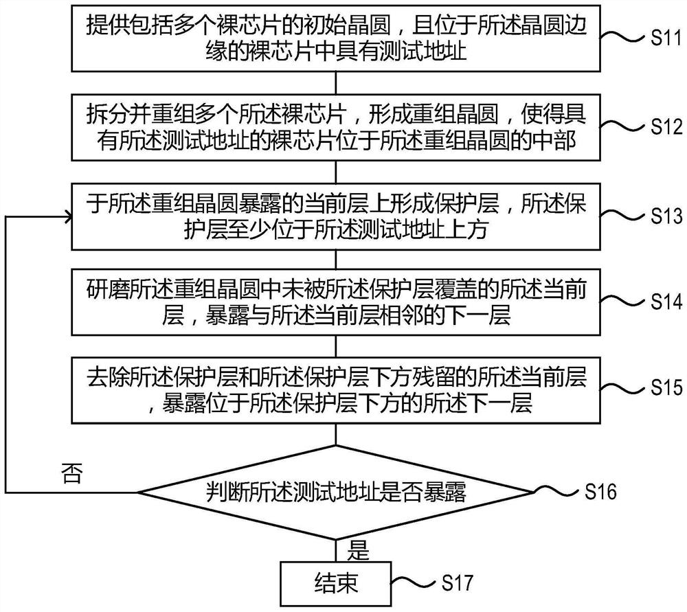
[0048] The specific implementations of the wafer grinding method and the wafer failure analysis method provided by the present invention will be described in detail below in conjunction with the accompanying drawings.
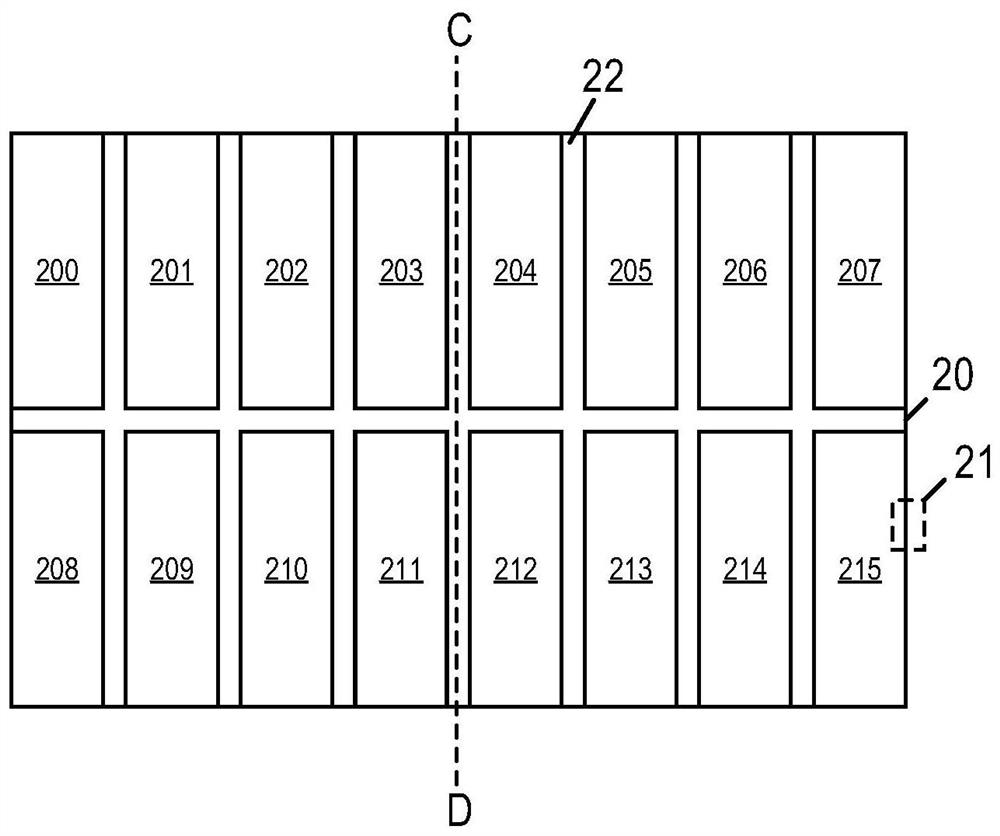
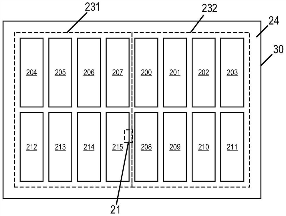
[0049] This specific embodiment provides a wafer grinding method, with figure 1 It is the flow chart of wafer grinding method in the specific embodiment of the present invention, appended Figures 2A-2H It is the main schematic diagram in the process of grinding the wafer according to the specific embodiment of the present invention. Such as figure 1 , Figure 2A-Figure 2H As shown, the wafer grinding method provided in this specific embodiment includes the following steps:
[0050] Step S11, providing an initial wafer 20 comprising a plurality of bare chips, and the bare chips located on the edge of the initial wafer 20 have a test address 21, such as Figure 2A shown.
[0051] Specifically, the initial wafer 20 has a plurality of bare chips arranged in a...
PUM
 Abstract
Description
Claims
Application Information
 - R&D Engineer
- R&D Manager
- IP Professional
- Industry Leading Data Capabilities
- Powerful AI technology
- Patent DNA Extraction
Browse by: Latest US Patents, China's latest patents, Technical Efficacy Thesaurus, Application Domain, Technology Topic.
© 2024 PatSnap. All rights reserved.Legal|Privacy policy|Modern Slavery Act Transparency Statement|Sitemap