Manufacturing method of embedded graphene diode
A manufacturing method and graphene technology, applied in semiconductor/solid-state device manufacturing, electrical components, circuits, etc., can solve problems such as excessive electrode current, PN junction breakdown, and unfavorable normal operation of diodes, so as to improve breakdown voltage, The effect of preventing breakdown
- Summary
- Abstract
- Description
- Claims
- Application Information
AI Technical Summary
Problems solved by technology
Method used
Image

Examples
Embodiment Construction
[0026] The mosaic graphene diode according to the disclosed embodiments of the present invention will be described in detail below with reference to the accompanying drawings.
[0027] As previously mentioned, the present invention provides a method for manufacturing a mosaic graphene diode, comprising:
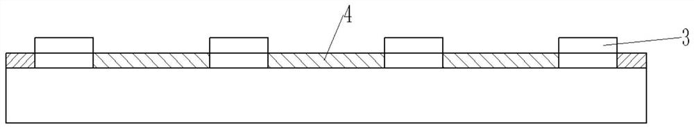
[0028] (1) provide a copper substrate;
[0029] (2) depositing a nickel metal layer on the copper substrate;
[0030] (3) forming a first mask layer on the nickel metal layer, the first mask layer having a plurality of first openings arranged in an array;
[0031] (4) Doping the nickel metal layer with first-type ions through the first mask layer to form first-type regions corresponding to a plurality of first openings;
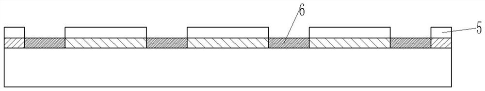
[0032] (5) remove the first mask layer, and form a second mask layer on the nickel metal layer, the second mask layer exposes other parts of the nickel metal layer except the first type region area;
[0033] (6) Doping the nickel metal layer with second-...
PUM
| Property | Measurement | Unit |
|---|---|---|
| thickness | aaaaa | aaaaa |
Abstract
Description
Claims
Application Information
 - R&D Engineer
- R&D Manager
- IP Professional
- Industry Leading Data Capabilities
- Powerful AI technology
- Patent DNA Extraction
Browse by: Latest US Patents, China's latest patents, Technical Efficacy Thesaurus, Application Domain, Technology Topic.
© 2024 PatSnap. All rights reserved.Legal|Privacy policy|Modern Slavery Act Transparency Statement|Sitemap