Inverted light-emitting diode

A light-emitting diode, flip-chip technology, applied in the direction of electrical components, circuits, semiconductor devices, etc., can solve the problems of increased resistance, increased electrode light absorption, light blocking area, and reduced antistatic ability

Pending Publication Date: 2021-09-07
QUANZHOU SANAN SEMICON TECH CO LTD
View PDF12 Cites 1 Cited by
  • Summary
  • Abstract
  • Description
  • Claims
  • Application Information

AI Technical Summary

Problems solved by technology

The reduction of antistatic ability is due to the reduction of the size of the light-emitting diode chip, the increase of its resistance, and the reduction of its own capacitance. The decrease in brightness and other performance is due to the need to set a larger area of ​​​​metal electrodes to reduce the resistance in order to enhance the antistatic ability as much as possible. , Increase the capacitance, but also increase the light absorption and light blocking area of ​​the electrode

Method used


Image

  • Inverted light-emitting diode
  • Inverted light-emitting diode
  • Inverted light-emitting diode

Examples


Embodiment 1

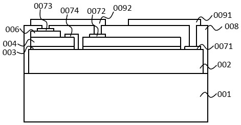
[0030] attached figure 1 A flip-chip light emitting diode is shown, which has a transparent substrate 001, a first semiconductor layer 002, a light emitting layer 003, a second semiconductor layer 004, a third semiconductor layer 006, the third semiconductor layer 006 is etched, the second semiconductor layer 004 The luminescent layer 003 forms three independent regions; the third semiconductor layer 006, the second semiconductor layer 004 and the luminescent layer 003 of the first region I are etched away to expose the first semiconductor layer 002; the second semiconductor layer 002 of the second region II is etched away The third semiconductor layer 006, exposing the second semiconductor layer 004; etching and removing part of the third semiconductor layer 006 in the third region III, exposing part of the second semiconductor layer 004; setting the first semiconductor layer 002 on the surface of the first region I A contact electrode 0071, a second contact electrode 0072 on...

Embodiment 2

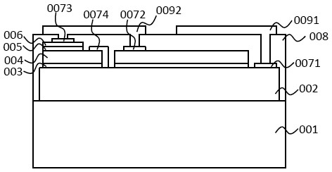
[0043] attached Figure 11 Another flip-chip light-emitting diode is shown, which has a transparent substrate 001, a first semiconductor layer 002, a light-emitting layer 003, a second semiconductor layer 004, a contact layer 0041, a barrier layer 005, a third semiconductor layer 006, and the third semiconductor layer is etched. The semiconductor layer 006, the barrier layer 005, the contact layer 0041, the second semiconductor layer 004 and the light emitting layer 003 form three independent regions; the third semiconductor layer 006 in the first region I, the barrier layer 005, the contact layer 0041, The second semiconductor layer 004 and the light emitting layer 003, exposing the first semiconductor layer 002; etching and removing the third semiconductor layer 006, barrier layer 005 and part of the contact layer 0041 in the second region II, exposing the second semiconductor layer 004 and the contact layer 0041; Part of the third semiconductor layer and the second semicond...

Embodiment 3

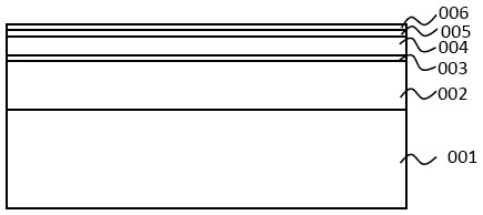
[0046] attached image 3 Another flip-chip light-emitting diode of the present invention is shown, which has a transparent substrate 001, a first semiconductor layer 002, a light-emitting layer 003, a second semiconductor layer 004, and a third semiconductor layer 006; the third semiconductor layer in this embodiment 006 is formed on the upper surface of the second semiconductor layer 004 by diffusion technology. Etching the third semiconductor layer 006, the second semiconductor layer 004, and the light-emitting layer 003 to form three independent regions; etching and removing the third semiconductor layer 006, the second semiconductor layer 004, and the light-emitting layer 003 in the first region I, exposing the first The semiconductor layer 002; etching and removing the third semiconductor layer 006 in the second region II, exposing the second semiconductor layer 004; etching and removing part of the third semiconductor layer 006 in the third region III, exposing part of t...


PUM

PropertyMeasurementUnit
thicknessaaaaaaaaaa
thicknessaaaaaaaaaa
thicknessaaaaaaaaaa

Abstract

The invention discloses a flip light-emitting diode, and the light-emitting diode comprises a transparent substrate, a first semiconductor layer, a light-emitting layer, a second semiconductor layer and a third semiconductor layer, three mutually independent areas are formed; the first region exposes the first semiconductor layer; the third semiconductor layer in the second region is etched and removed to expose the second semiconductor layer; a part of the third semiconductor layer in the third region is etched and removed to expose a part of the second semiconductor layer; a first contact electrode is arranged on the surface of the first semiconductor layer in the first region, a second contact electrode is arranged on the surface of the second semiconductor layer in the second region, and a third contact electrode and a fourth contact electrode are arranged on the surfaces of the third semiconductor layer and the second semiconductor layer in the third region; the fourth contact electrode is connected with the first semiconductor layer at the same time. The light-emitting diode also comprises a first metal welding layer which is electrically connected with the first contact electrode, and a second metal welding layer which is electrically connected with the second contact electrode and the third contact electrode. The flip light-emitting diode has the advantages of high brightness, strong antistatic capability and the like.

Description

technical field [0001] The invention relates to a flip-chip light-emitting diode, which belongs to the field of semiconductor optoelectronic devices and technologies. Background technique [0002] Light Emitting Diode (LED for short) has the advantages of high luminous intensity, high efficiency, small size, and long service life, and is considered to be one of the most potential light sources at present. In recent years, LEDs have been widely used in daily life, such as lighting, signal display, backlight, car lights, and large-screen displays. At the same time, these applications also put forward higher requirements for the brightness and luminous efficiency of LEDs. [0003] Flip-chip light-emitting diodes have the advantages of high brightness, good heat dissipation, and small package size, and are especially suitable for LED displays with ultra-high pixel density. With the improvement of technology and consumer demand, the pixel density of LED display is getting higher...

Claims


Application Information

Patent Timeline
Patent Type & Authority Applications(China)
IPC IPC(8): H01L33/02H01L33/14H01L33/36H01L33/62
CPCH01L33/02H01L33/14H01L33/36H01L33/62
Inventor 熊伟平王鑫吴志伟高迪彭钰仁郭桓邵
Owner QUANZHOU SANAN SEMICON TECH CO LTD
Why Eureka
Try Eureka