Electromagnetic absorption structure with wide incident angle
A technology of incident angle and absorption structure, applied in the direction of electrical components, antennas, etc., can solve problems such as increasing complexity
- Summary
- Abstract
- Description
- Claims
- Application Information
AI Technical Summary
Problems solved by technology
Method used
Image
Examples
Embodiment
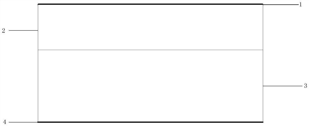
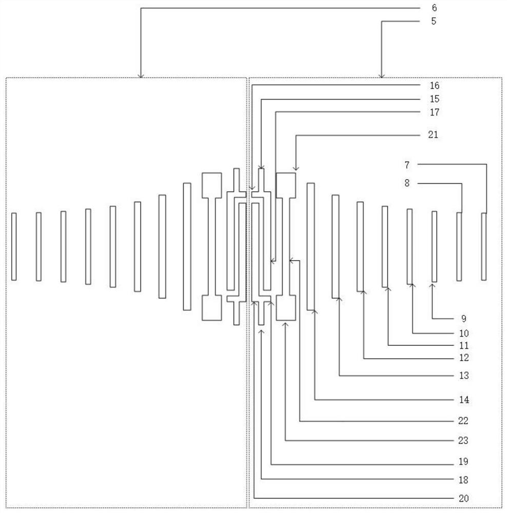
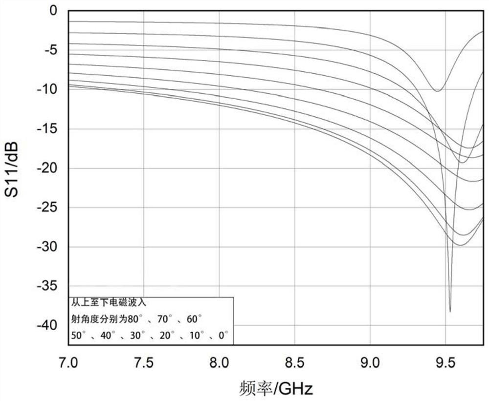
[0018] Example: such as figure 1 and figure 2 As shown, an electromagnetic absorption structure with a wide incident angle, including ITO (smoke tin oxide) pattern layer 1, substrate 2, dielectric loss layer 3 and good conductor layer 4 laminated from top to bottom, substrate 2, dielectric loss layer 3 And the good conductor layer 4 is a rectangular plate respectively, and the substrate 2, the dielectric loss layer 3 and the good conductor layer 4 are completely overlapped from top to bottom; the ITO pattern layer 1 is composed of a first ITO structure 5 and a second ITO structure 6, and the first Both the ITO structure 5 and the second ITO structure 6 are attached to the upper surface of the substrate 2. The first ITO structure 5 includes a first rectangular ITO7, a second rectangular ITO8, a third rectangular ITO9, a fourth rectangular ITO10, a fifth rectangular ITO11, a Sixth rectangle ITO12, seventh rectangle ITO13, eighth rectangle ITO14, ninth rectangle ITO15, tenth re...
PUM
| Property | Measurement | Unit |
|---|---|---|
| Length | aaaaa | aaaaa |
| Width | aaaaa | aaaaa |
| Thickness | aaaaa | aaaaa |
Abstract
Description
Claims
Application Information


