Eureka AIR delivers breakthrough ideas for toughest innovation challenges, trusted by R&D personnel around the world.

PCB character ink-jet nano color paste as well as preparation method and application thereof

A nano-color paste and character technology, applied in applications, inks, household appliances, etc., can solve the problems of easy falling off and poor stability of PCB board ink, and achieve the effects of not easy falling off, excellent anti-settling performance and excellent performance.

Inactive Publication Date: 2021-09-24
深圳市墨库图文技术有限公司
View PDF2 Cites 2 Cited by
  • Summary
  • Abstract
  • Description
  • Claims
  • Application Information

AI Technical Summary

Problems solved by technology

[0005] The purpose of this application is to provide a PCB character inkjet nano-color paste and its preparation method and application, aiming to solve the problem of poor stability and easy falling off of PCB ink used for inkjet processing in the prior art

Method used


Image

  • PCB character ink-jet nano color paste as well as preparation method and application thereof
  • PCB character ink-jet nano color paste as well as preparation method and application thereof
  • PCB character ink-jet nano color paste as well as preparation method and application thereof

Examples


preparation example Construction

[0047] The second aspect of the embodiment of the present application provides a method for preparing a PCB character inkjet nano-color paste, including the following steps:

[0048] S01. Provide various components according to the PCB character inkjet nano-color paste;

[0049] S02. Performing the first mixing treatment on the acrylate monomer, dispersant and auxiliary agent to obtain the first mixture;

[0050] S03. performing a second mixing treatment on the first mixture, titanium dioxide, and aluminum hydroxide to obtain a second mixture;

[0051] S04. The second mixture is sequentially subjected to grinding treatment and filtration treatment to obtain PCB character inkjet nano color paste.

[0052] The preparation method of the PCB character inkjet nano-color paste provided by the second aspect of the present application, the preparation method is through mixing each component, and then performing grinding treatment and filtering treatment, so as to ensure that the PCB ...

Embodiment 1

[0066] PCB character ink-jet nano color paste and its preparation method and PCB ink-jet ink

[0067] PCB character inkjet nano color paste

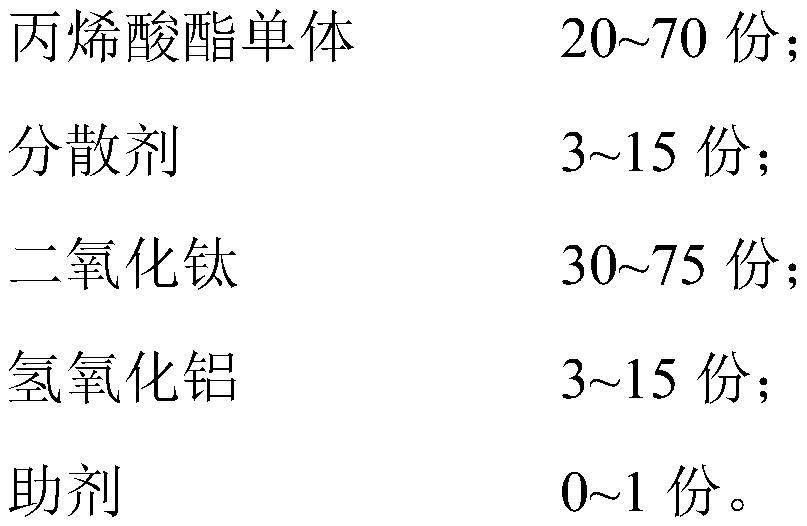
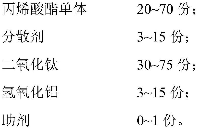
[0068] The PCB character inkjet nano color paste includes the following components in parts by weight:

[0069]

[0070] Preparation method of PCB character inkjet nano color paste

[0071] Provide various components according to PCB character inkjet nano color paste;

[0072] Perform the first mixing treatment on the acrylate monomer, dispersant and auxiliary agent under the condition of 200-400 rpm for 0.5-1 hour to obtain the first mixture;

[0073] performing a second mixing treatment on the first mixture, titanium dioxide, and aluminum hydroxide at 300-600 rpm for 2 hours to obtain a second mixture;

[0074] Grinding and filtering the second mixture in turn to obtain PCB character inkjet nano-color paste; grinding treatment is to provide ceramic nano-sand mill and zirconium beads for grinding, wherein the filling amount of ...

Embodiment 2

[0078] PCB character ink-jet nano color paste and its preparation method and PCB ink-jet ink

[0079] PCB character inkjet nano color paste

[0080] Among the titanium dioxide components included in the PCB character inkjet nano-color paste, there are 20 parts of Lomon Billions TR52 and 30 parts of Sahaliben RM300. The other components and preparation method of PCB character inkjet nano-color paste are consistent with those in Example 1.

[0081] PCB inkjet ink

[0082] The PCB inkjet ink includes the PCB character inkjet nano-color paste provided in Example 2.


PUM

PropertyMeasurementUnit
particle diameteraaaaaaaaaa

Abstract

The invention provides a PCB character ink-jet nano color paste, and the paste comprises the following components: 20-70 parts of acrylate monomer; 3-15 parts of a dispersing agent; 30-75 parts of titanium dioxide; 3-15 parts of aluminum hydroxide; and 0-1 part of an auxiliary agent. According to the color paste, the acrylate monomer is used as a main component and cooperates with the dispersing agent, the titanium dioxide and the aluminum hydroxide to act, and based on the synergistic effect of the titanium dioxide and the aluminum hydroxide, the adhesiveness of the acrylate monomer can be improved, the stability and the anti-settling property of the obtained PCB character ink-jet nano color paste are improved, the excellent performance of the color paste is ensured, the service life is prolonged, and the paste is not prone to falling off in the using process, does not have the layering or bottom sinking phenomenon after being aged at high temperature for 14 days, is excellent in smoothness on a machine, and is beneficial to wide application.

Description

technical field [0001] The application belongs to the technical field of PCB inkjet ink, and in particular relates to a PCB character inkjet nano color paste and its preparation method and application. Background technique [0002] The preparation process of the PCB board includes the following steps: (1) printing the circuit board; (2) cutting the copper clad laminate; (3) pretreating the copper clad laminate; (4) transferring the circuit board; (5) corroding the circuit board; (6) wiring Board drilling; (7) circuit board pretreatment to obtain the PCB board. In the process of PCB board manufacturing, the most critical thing is to arrange electronic circuits on the copper clad board. Only when the circuit layout is correctly realized on the surface of the PCB board can it play a corresponding role. [0003] At present, the design of electronic circuits is basically realized by etching on copper clad laminates, so circuit etching is a very critical step, and the effect of c...

Claims


Application Information

Patent Timeline
Patent Type & Authority Applications(China)
IPC IPC(8): C09D11/322C09D17/00
CPCC09D17/008C09D17/007C09D11/322
Inventor 钟衍明明亚强范晓华周孝远
Owner 深圳市墨库图文技术有限公司
Why Eureka
Eureka Blog
Learn More