Chip testing method and device

A technology of chip testing and test conditions, applied in semiconductor/solid-state device testing/measurement, electrical components, circuits, etc., can solve problems such as yield loss and achieve the effect of improving output yield

Active Publication Date: 2021-10-08
HYGON INFORMATION TECH CO LTD
View PDF7 Cites 1 Cited by
  • Summary
  • Abstract
  • Description
  • Claims
  • Application Information

AI Technical Summary

Problems solved by technology

[0004] In related technologies, when testing the die on the wafer, no matter wheth

Method used


Image

  • Chip testing method and device
  • Chip testing method and device
  • Chip testing method and device

Examples


Embodiment Construction

[0043] Embodiments of the present invention will be described in detail below in conjunction with the accompanying drawings.

[0044] It should be clear that the described embodiments are only some of the embodiments of the present invention, not all of them. Based on the embodiments of the present invention, all other embodiments obtained by persons of ordinary skill in the art without creative efforts fall within the protection scope of the present invention.

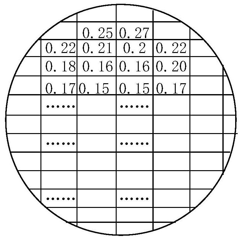
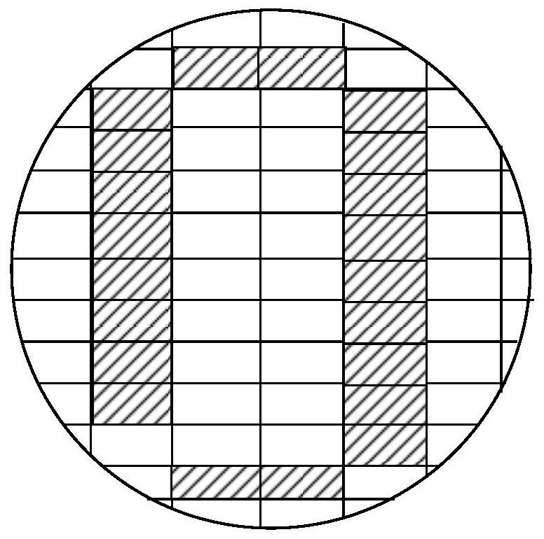
[0045] As mentioned in the background, in the field of semiconductor processing, grain failures can generally be classified into two types: hard failure and soft failure. Among them, hard failure is mainly reflected in the short circuit or open circuit of semiconductor devices or metal interconnection layers in the grain due to process defects, and the complete loss of grain function. Soft failure is mainly reflected in the deviation of the electrical characteristics of the semiconductor device in the grain, beyond t...


PUM


Abstract

The embodiment of the invention discloses a chip testing method and device, which relate to the technical field of semiconductor processing, and can effectively improve the yield of crystal grains. The method comprises the following steps of according to a preset rule, selecting at least one part of invalid crystal grains obtained by a mass production test to obtain alternative crystal grains, carrying out an additional test on the alternative crystal grains, wherein the test condition of the additional test is different from the test condition of the mass production test, and in response to the alternative crystal grain passing the additional test, appointing an application scene corresponding to a test condition of the additional test for the alternative crystal grain to obtain a target crystal grain. The method is suitable for chip testing.

Description

technical field [0001] The invention relates to the technical field of semiconductor processing, in particular to a chip testing method and device. Background technique [0002] In the semiconductor manufacturing process, since the process conditions in the reaction chamber are not exactly the same (for example, the process conditions at the edge of the wafer and the center of the wafer are different), the specific process parameters of different dies (die) on the same wafer There are also differences, resulting in certain deviations in the performance of each grain, and even some grains may not be able to achieve their expected functions, resulting in grain failure. [0003] Grain failure can generally be divided into two types: hard failure (hard fail) and soft failure (soft fail). Among them, hard failure is mainly reflected in the short circuit or open circuit of semiconductor devices or metal interconnection layers in the grain due to process defects, and the complete ...

Claims


Application Information

Patent Timeline
IPC IPC(8): H01L21/66
CPCH01L22/20H01L22/26
Inventor 洪波
Owner HYGON INFORMATION TECH CO LTD
Why Eureka
Try Eureka