Transient voltage suppression protection device with latticed cathode and anode groove structures
A technology for transient voltage suppression and protection devices, which is applied in the direction of electric solid state devices, electrical components, semiconductor devices, etc., can solve the problems of easy-to-cause latch-up, device current capacity drop, etc., so as to alleviate current concentration, improve device current capacity, The effect of maintaining the voltage rise
- Summary
- Abstract
- Description
- Claims
- Application Information
AI Technical Summary
Problems solved by technology
Method used
Image
Examples
Embodiment 1
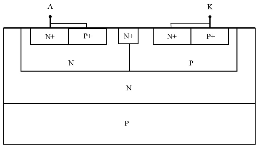
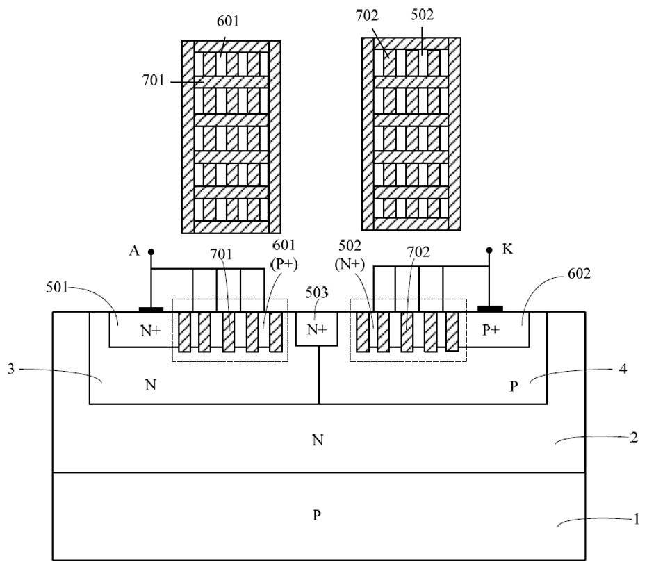
[0017] Such as figure 2 As shown, the embodiment of the present invention proposes a transient voltage suppression protection device (referred to as the device in this application) with a grid-like cathode and anode trench structure, including: a P-type substrate 1, on which a P-type substrate 1 An N-type epitaxy 2 is grown; an N-type well region 3 is formed on the upper left side of the N-type epitaxy 2, and a P-type well region 4 tangential to the N-type well region 3 is formed on the upper right side of the N-type epitaxy 2; A first N+ region 501 is formed on the left side below the surface of the P-type well region 3, and a first P+ region 601 tangent to the right side of the first N+ region 501 is formed on the right side; A second N+ region 502 is formed on the side, and a second P+ region 602 tangent to the right side of the second N+ region 502 is formed on the right side; a third N+ region is formed at the junction of the N-type well region 3 and the P-type well regi...
Embodiment 2
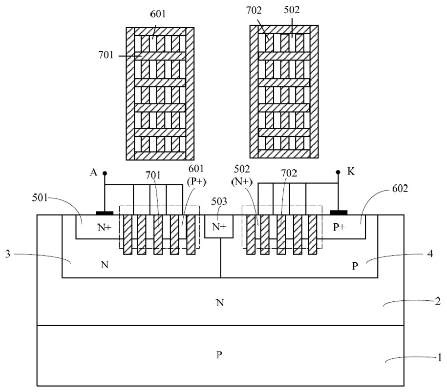
[0024] Such as image 3 As shown, the groove depths of the first groove structure 701 and the second groove structure 702 in the second embodiment are deeper than those in the first embodiment;
[0025] In the second embodiment, the current of the device is distributed more uniformly in each grid through deeper grooves, and at the same time, the path of the device current in the vertical direction is further increased, the amplification factor of the parasitic transistor in the SCR device is further reduced, and the sustaining voltage Vh is increased. , to avoid latch-up effect.
PUM
 Abstract
Description
Claims
Application Information
 - R&D
- Intellectual Property
- Life Sciences
- Materials
- Tech Scout
- Unparalleled Data Quality
- Higher Quality Content
- 60% Fewer Hallucinations
Browse by: Latest US Patents, China's latest patents, Technical Efficacy Thesaurus, Application Domain, Technology Topic, Popular Technical Reports.
© 2025 PatSnap. All rights reserved.Legal|Privacy policy|Modern Slavery Act Transparency Statement|Sitemap|About US| Contact US: help@patsnap.com


