Preparation method of insulated gate bipolar transistor

A technology of bipolar transistors and insulated gates, applied in semiconductor/solid-state device manufacturing, electrical solid-state devices, semiconductor devices, etc., can solve the problems of easy fragmentation, expensive equipment, and easy rupture, so as to reduce fragmentation and eliminate cracking Effect

Pending Publication Date: 2021-10-15
SHANGHAI FINE CHIP SEMICON
View PDF4 Cites 0 Cited by
  • Summary
  • Abstract
  • Description
  • Claims
  • Application Information

AI Technical Summary

Problems solved by technology

[0006] The Taiko process has the following disadvantages: the Taiko process only uses a thick edge with a width of 2-4mm to support the wafer without warping, but the wafer itself is still a thin sheet, and it is still easy to break in subsequent processing; Taiko thinning equipment and subsequent equipment

Method used


Image

  • Preparation method of insulated gate bipolar transistor
  • Preparation method of insulated gate bipolar transistor
  • Preparation method of insulated gate bipolar transistor

Examples


Embodiment Construction

[0025] The present invention will be further described below in conjunction with the accompanying drawings and specific embodiments.

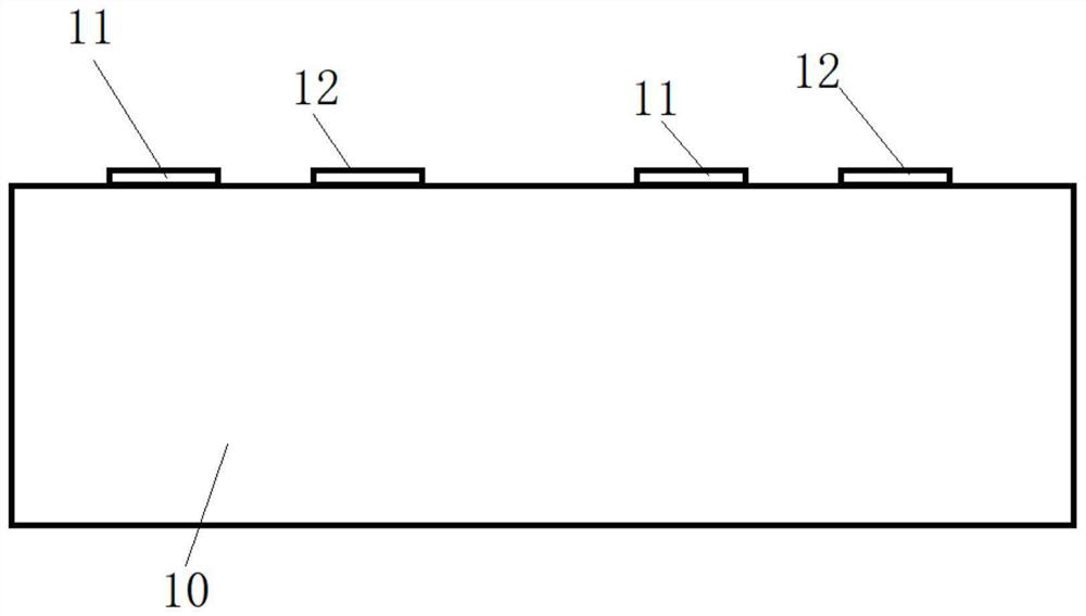
[0026] see Figure 3 to Figure 8 , the preparation method of the insulated gate bipolar transistor of the present invention, after finishing the front process of the IGBT wafer, make the bump 20 on the pressure pads of the collector 11 and the gate 12 on the front side of the wafer 10 (see image 3 and Figure 4 ); the bump 20 is a copper pillar (Cu Pillar), a gold pillar (Gold Pillar) or a solder ball (Solder Ball). If it is a copper pillar (Cu pillar) or a gold pillar (Gold pillar), the height range of the copper pillar (Cu pillar) or gold pillar (Gold pillar) is 10-100um. If it is a solder ball (Solder Ball), the diameter of the solder ball is 50-400um.

[0027] see Figure 5 , and then perform wafer-level plastic sealing on the front side of the wafer 10 to form a plastic sealing layer 30, the thickness of the resin of the plastic seali...


PUM

PropertyMeasurementUnit
Diameteraaaaaaaaaa
Thicknessaaaaaaaaaa

Abstract

The invention discloses a preparation method of an insulated gate bipolar transistor (IGBT), which is characterized by comprising the following steps of: manufacturing bumps on pressure welding points of a collector electrode and a grid electrode on the front surface of a wafer after the front surface of the IGBT wafer is manufactured; performing wafer-level plastic package on the front surface of the wafer to form a plastic package layer; grinding the plastic package layer to expose the previously manufactured bump; and finally, carrying out back surface processing; or performing a back surface manufacturing process firstly, and then grinding the plastic package layer to expose the previously manufactured bumps. According to the method, temporary bonding is not needed, and the problems of wafer breakage and the like caused by temporary bonding stripping are eliminated; and meanwhile, the plastic packaging layer is always on the front surface of the wafer, so that the wafer is always a thick wafer in the back surface processing process, and the problems of wafer breakage and the like can be reduced.

Description

technical field [0001] The invention relates to the technical field of transistors, in particular to a preparation method of an insulated gate bipolar transistor. Background technique [0002] IGBT (Insulated Gate Bipolar Transistor), Insulated Gate Bipolar Transistor, is a composite fully-controlled voltage-driven power semiconductor device composed of BJT (Bipolar Transistor) and MOS (Insulated Gate Field Effect Transistor), with MOSFET The advantages of high input impedance and low conduction voltage drop of GTR. The saturation voltage of GTR is low, the carrying current density is large, but the driving current is large; the driving power of MOSFET is small, the switching speed is fast, but the conduction voltage drop is large, and the current carrying density is small. The IGBT combines the advantages of the above two devices, with low driving power and low saturation voltage. It is very suitable for the conversion system with a DC voltage of 600V and above, such as A...

Claims


Application Information

Patent Timeline
IPC IPC(8): H01L21/60
CPCH01L24/81H01L2224/0812
Inventor 黄平鲍利华顾海颖
Owner SHANGHAI FINE CHIP SEMICON
Why Eureka
Try Eureka