Design method of dual-band spin selective transmission metasurface device
A device design and metasurface technology, applied to electrical components, antennas, etc., to reduce processing difficulty and save production costs
- Summary
- Abstract
- Description
- Claims
- Application Information
AI Technical Summary
Problems solved by technology
Method used
Image

Examples
Embodiment 1
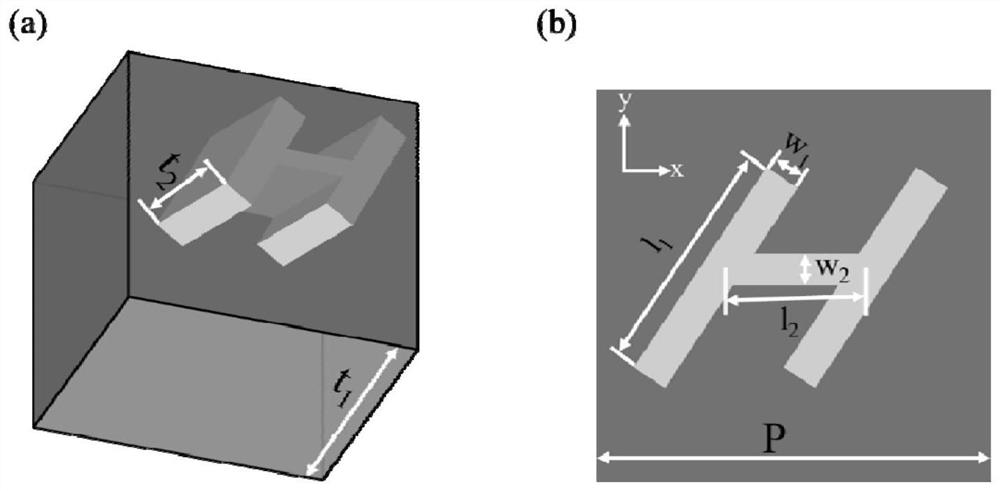
[0020] Example 1, refer to figure 1 , the design method of the dual-band spin-selective transmission metasurface device of this scheme specifically includes the following steps:
[0021] S1. Design the basic structure so that the basic structure can realize the spin-selective transmission of dual frequency bands.
[0022] S2. The basic structures designed in step 1 are arranged periodically.
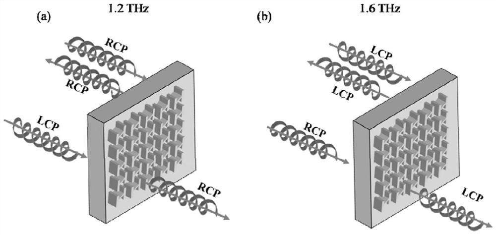
[0023] The above designs are all based on high-resistance silicon with a thickness of 500 μm. The basic structure described in step 1 is an H-type medium column. In the present invention, the metasurface works in the frequency band around 1.2 and 1.6 THz, and the total thickness of silicon is t 1 +t 2 =500μm, the etching height of the dielectric column is t 2 = 200 μm, the length of the rectangular strips on both sides of the dielectric column is l 1 =70μm, width is w 1 = 22 μm and an angle of 45° with the x-axis. The center-to-center spacing of the rectangular bars on both sides...
Embodiment 2
[0024] The second embodiment specifically includes:
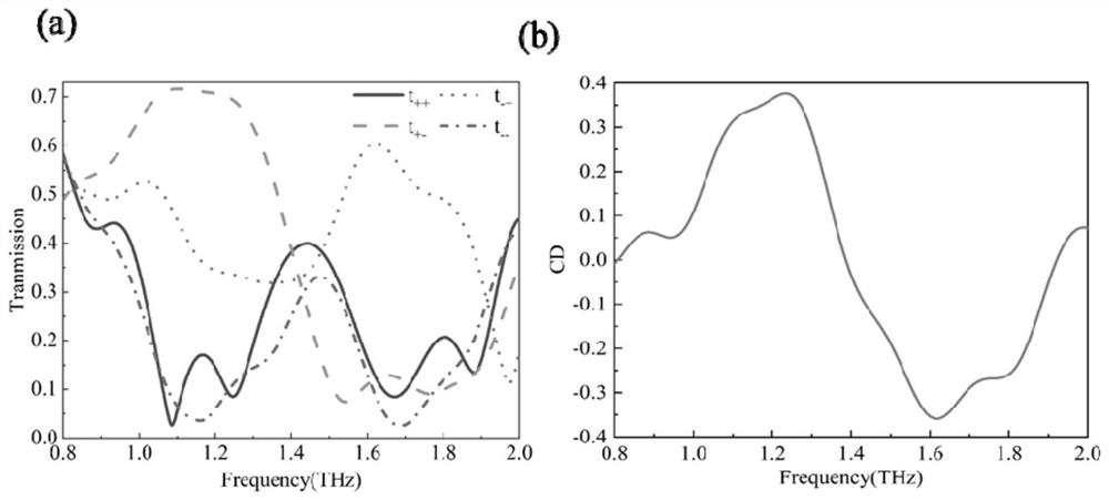
[0025] S1. Design the basic structure so that the basic structure can realize the spin-selective transmission of dual frequency bands. like figure 1 As shown, the basic structure is an H-type dielectric column. In the present invention, the metasurface works in the frequency band around 1.2 and 1.6 THz, and is determined by figure 1 (a) It can be seen that the total thickness of silicon is t 1 +t 2 =500μm, the etching height of the dielectric column is t 2 = 200 μm. figure 1 (b) is a top view of the unit. The length of the rectangular strips on both sides of the dielectric column is l 1 =70μm, width is w 1 = 22 μm and an angle of 45° with the x-axis. The center-to-center spacing of the rectangular bars on both sides of the dielectric column is l 2 = 90 μm, the width of the column connecting the rectangular bars on both sides is w 2 = 16 μm. The period of the entire cell is P=150 μm. like figure 2 (a), "+" and...
PUM
| Property | Measurement | Unit |
|---|---|---|
| Thickness | aaaaa | aaaaa |
| Width | aaaaa | aaaaa |
Abstract
Description
Claims
Application Information
 - R&D
- Intellectual Property
- Life Sciences
- Materials
- Tech Scout
- Unparalleled Data Quality
- Higher Quality Content
- 60% Fewer Hallucinations
Browse by: Latest US Patents, China's latest patents, Technical Efficacy Thesaurus, Application Domain, Technology Topic, Popular Technical Reports.
© 2025 PatSnap. All rights reserved.Legal|Privacy policy|Modern Slavery Act Transparency Statement|Sitemap|About US| Contact US: help@patsnap.com