
Automatic assembling machine for inlaid ceramic chips

An automatic assembly machine and ceramic chip technology, applied in packaging, transportation and packaging, heating and unsealing, etc., can solve the problems of difficult control of precision, unqualified product quality, heavy workload, etc., to improve automation level and production efficiency, meet Automated production line, the effect of improving work efficiency

Inactive Publication Date: 2021-10-22
苏州达文西自动化科技有限公司
View PDF0 Cites 1 Cited by
  • Summary
  • Abstract
  • Description
  • Claims
  • Application Information

AI Technical Summary

Problems solved by technology

If manual operation is used, the ceramic pieces after cutting are relatively small, not easy to tear off, and it is easy to be tired after long-term operation, the workload is relatively large, and the efficiency is relatively low
[0006] On the other hand, there are many through-holes on the PCB, and the sizes of the through-holes on some PCBs are different. Each through-hole needs to place a corresponding ceramic chip. If it is placed manually, the efficiency is relatively low and the workload is relatively large. Large, the precision is not easy to control; moreover, manual operation takes a long time and is easy to be tired, and it will also be placed incorrectly, resulting in unqualified product quality and rework

Method used


Image

  • Automatic assembling machine for inlaid ceramic chips
  • Automatic assembling machine for inlaid ceramic chips
  • Automatic assembling machine for inlaid ceramic chips

Examples


Embodiment Construction

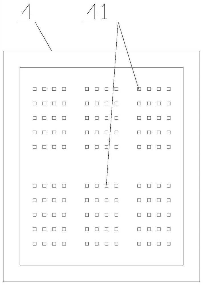
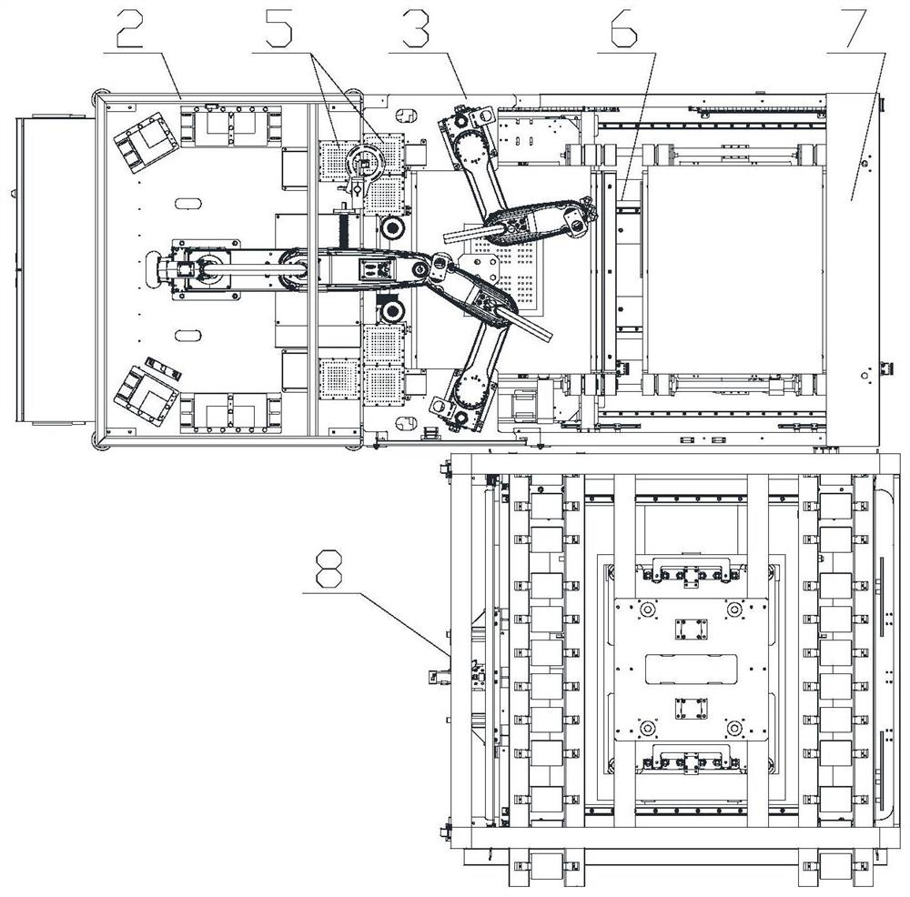
[0051] The present invention will be described in detail in conjunction with accompanying drawing now. This figure is a simplified schematic diagram only illustrating the basic structure of the present invention in a schematic manner, so it only shows the components relevant to the present invention.

[0052] Such as image 3 As shown, an automatic assembly machine for inlaid ceramic sheets of the present invention includes a ceramic sheet debonding and film tearing mechanism 2, a ceramic sheet visual inserting mechanism 3, a substrate exchange and replacement mechanism 6, and a substrate stacking mechanism arranged in sequence along the process 8. Among them, the ceramic sheet degumming and film tearing mechanism 2 is used for degumming and tearing off the adhesive film 1a on the back of the ceramic sheet slice 1, and is used for feeding and feeding the ceramic sheet visual inserting mechanism 3; The feeding mechanism 3 is used to embed the ceramic sheet 1b after the adhesiv...


PUM


Abstract

The invention provides an automatic assembling machine for inlaid ceramic chips. Theautomatic assembling machine comprises a ceramic chip peptizing and film tearing mechanism, a visual ceramic chip embedding mechanism, a substrate alternate material changing mechanism and a substrate laminating mechanism which are sequentially arranged along a working procedure, wherein the ceramic chip peptizing and film tearing mechanism is used for peptizing and tearing glue films on the back surfaces of ceramic chip slices, and feeding and supplying materials to the visual ceramic chip embedding mechanism; and the visual ceramic chip embedding mechanism is used for embedding the ceramic chip into the through hole of the PCB after the glue film of the ceramic chip is removed by the ceramic chip peptizing and film tearing mechanism, so that embedding of the ceramic chip is realized. Rapid dispergation and tearing of a glue film can be realized, the working efficiency is improved, and the requirements of an automatic production line are met; the sizes of the holes in the plate can be accurately recognized in a visual recognition mode, so that the accuracy of placing the ceramic chips is improved, manual discharging is converted into mechanical arm discharging, and the automation level and the production efficiency are improved.

Description

technical field [0001] The invention relates to the technical field of PCB board production equipment, in particular to an automatic assembly machine for inlaid ceramic sheets. Background technique [0002] The embedded ceramic chip in the PCB board is mainly designed to solve the problem of failure caused by the aging of the PCB itself due to heat dissipation and shortened life of the high-power heating components on the PCB during use. Therefore, it is necessary to correspond to high-power components on the PCB board. The position of the heating element is embedded in the ceramic sheet, and its position accuracy is relatively high (±0.005mm). This process is currently widely used in foreign mainstream automobile lamp factories. It is a necessary process for LED light source and laser light source PCB board. [0003] In the manufacturing process of the PCB board, at first, the heat dissipation requirements of the heating components on the PCB board determine the required si...

Claims


Application Information

Patent Timeline
IPC IPC(8): B25B27/00B65B69/00
CPCB25B27/00B65B69/0066
Inventor 唐亮辛惠显
Owner 苏州达文西自动化科技有限公司
Learn More