Cleaning device for chip wafer production

A technology for cleaning devices and wafers, which is applied in the manufacture of electrical components, semiconductor/solid-state devices, circuits, etc. It can solve problems such as waste of resources, damage to liquid medicine products, small size, etc., and achieve the effect of avoiding jitter and speeding up efficiency

Inactive Publication Date: 2021-10-22
安徽海之量储存设备有限公司
View PDF0 Cites 1 Cited by
  • Summary
  • Abstract
  • Description
  • Claims
  • Application Information

AI Technical Summary

Problems solved by technology

However, this cleaning method has too much impact on the chip, which is likely to cause damage to the component pattern, and the utilization rate of deionized water in this cleaning method is low, resulting in waste of resources
[0004] Chip wafer cleaning on the market also uses manual proportioning of the chemical solution, and then the chip wafer is cleaned by soaking in the chemical solution, ordinary drying, and additional baking. Although the process is simple, there are many problems. First, the chemical The liquid ratio is difficult to digitize, which has a great quality risk to product quality; secondly, it is difficult to meet the cleaning requirements of the chip wafer during the soaking process, and the residual liquid and the damage to the product are serious; thirdly, the chemical liquid cleaning tank There is a risk of secondary pollution to the chip wafer; the chip wafer after cleaning again cannot guarantee the drying of water and chemical solution, which will lead to serious residue; finally, after the traditional drying, the surface of the wafer will be left with water stains, resulting in traditional The cleaning efficiency and cleaning effect of the process are poor
[0005] Due to the large number of bumps on the surface of the chip, small size, and made of soft metal, it is easy to be scratched and damaged by tweezers during the cleaning process; optoelectronic device chips are usually made of some relatively brittle materials, which are extremely Easy to be damaged due to excessive clamping force, resulting in chip scrapping

Method used


Image

  • Cleaning device for chip wafer production
  • Cleaning device for chip wafer production
  • Cleaning device for chip wafer production

Examples


Embodiment Construction

[0032] The technical solutions of the present invention will be clearly and completely described below in conjunction with the embodiments. Apparently, the described embodiments are only some of the embodiments of the present invention, not all of them. Based on the embodiments of the present invention, all other embodiments obtained by persons of ordinary skill in the art without creative efforts fall within the protection scope of the present invention.

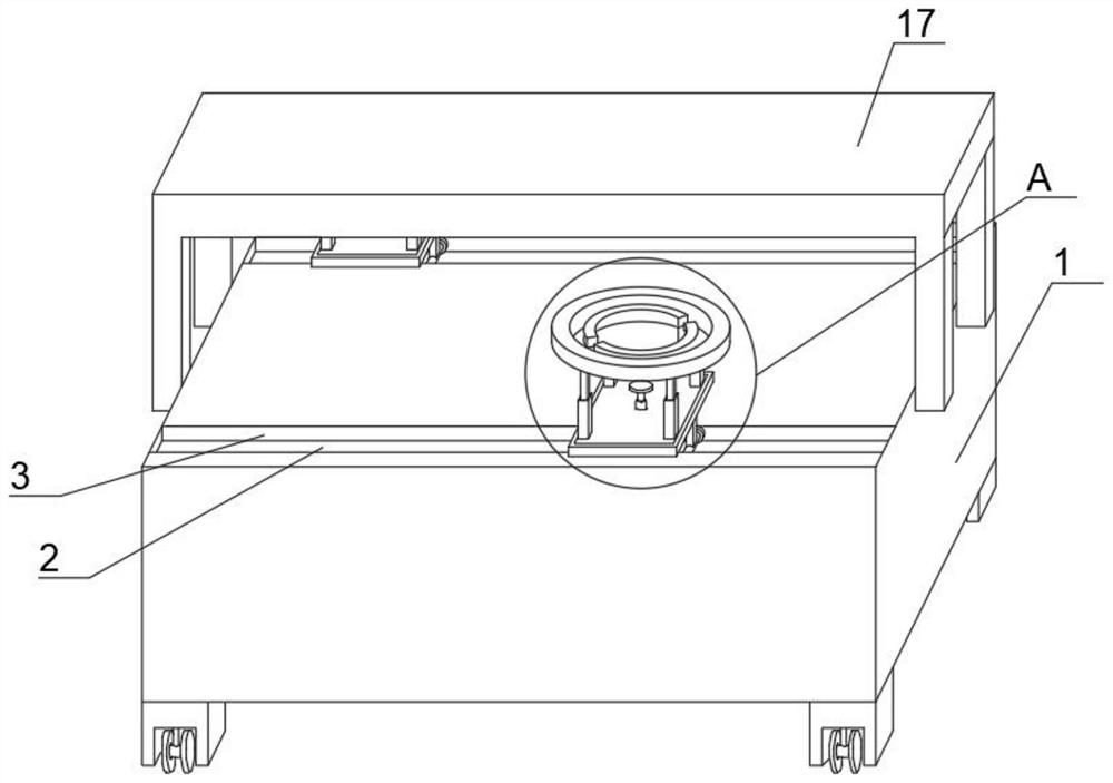
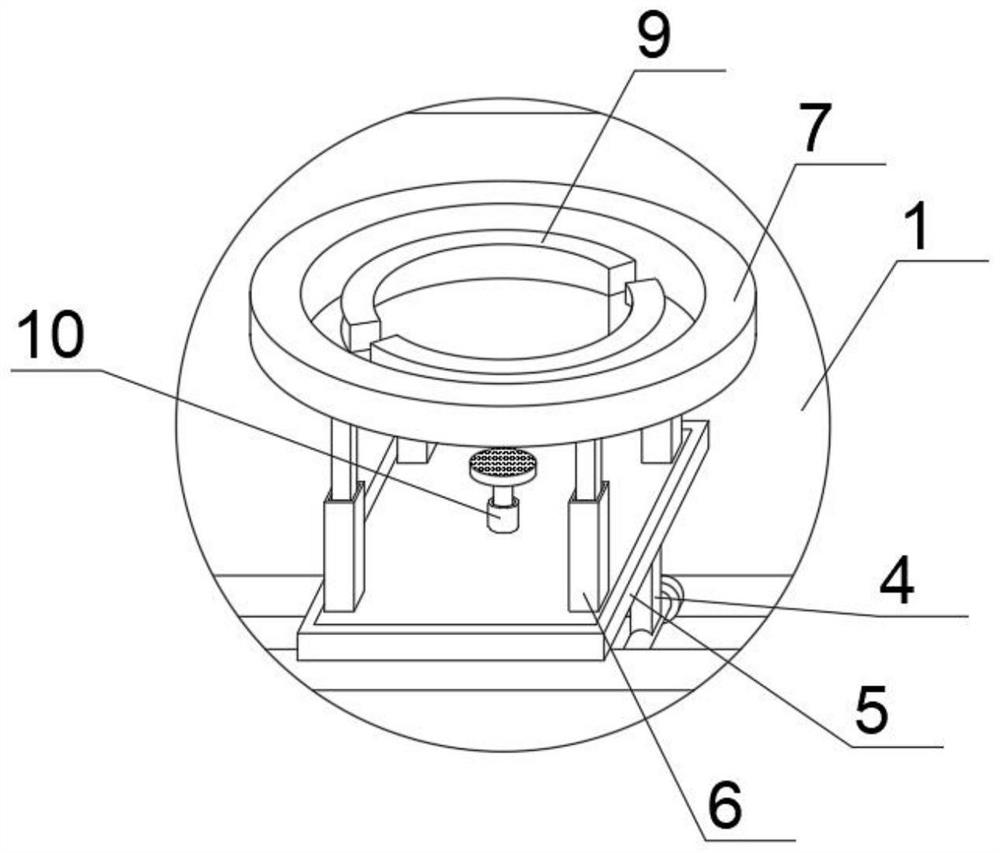
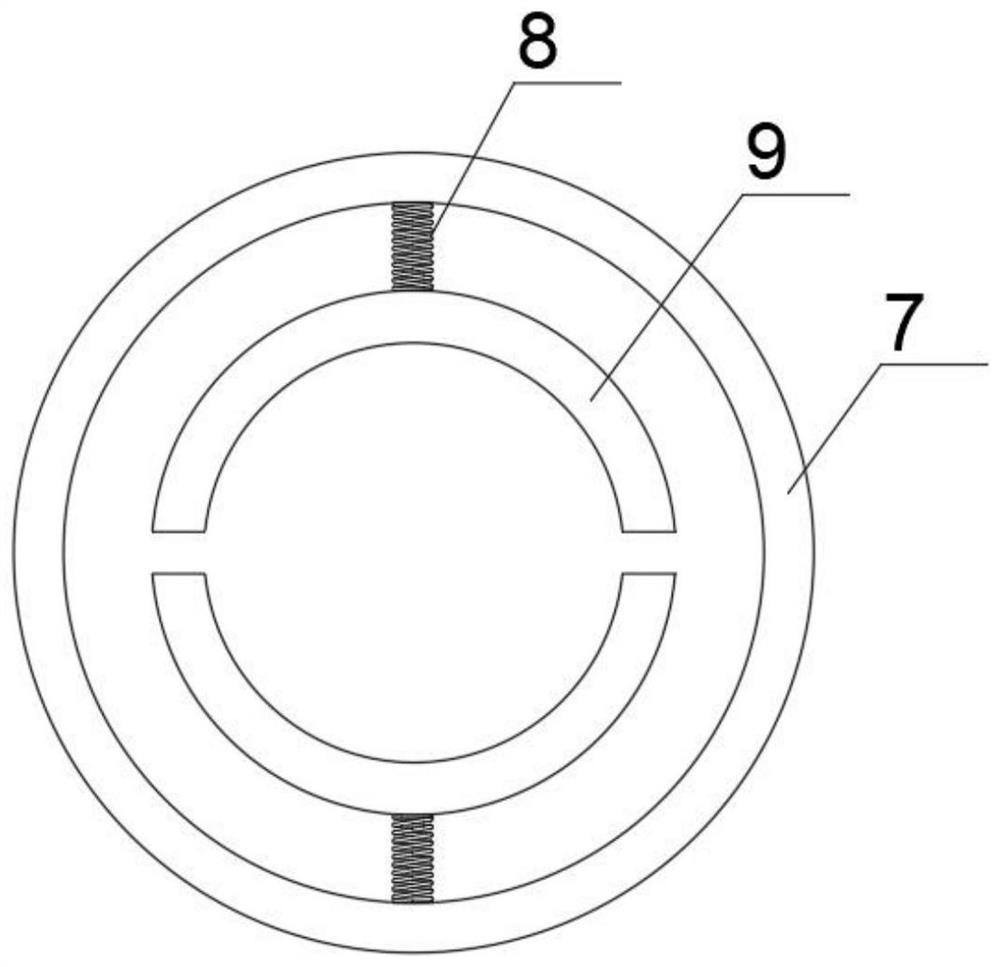
[0033] see Figure 1-7 As shown, a cleaning device for chip wafer production includes an operation table 1, a first chute 2 is symmetrically provided on the top surface of the operation table 1, and a second chute is symmetrically provided on the inner wall of the first chute 2 3. A number of rotating shafts are movable inside the first chute 2 on both sides, and the middle part of the rotating shaft is sleeved with a bushing, and the side of the bushing different from the first chute 2 is fixedly connected with a fixed rod...


PUM


Abstract

The invention discloses a cleaning device for chip wafer production, and belongs to the technical field of chip processing, wherein the cleaning device comprises an operation table; first sliding grooves are symmetrically formed in the top surface of the operation table, second sliding grooves are symmetrically formed in the inner walls of the first sliding grooves, and a plurality of rotating shafts are movably arranged in the first sliding grooves in the two sides; the middle of each rotating shaft is sleeved with a shaft sleeve, fixing rods are fixedly connected to the sides, different from the first sliding grooves, of the shaft sleeve, a bearing plate is fixed to the end faces, different from the shaft sleeve, of the two fixing rods, and a plurality of first electric telescopic rods are fixedly connected to the surface of the top of the bearing plate; the end faces of the telescopic ends of the four first electric telescopic rods are fixedly connected with sliding rings, and first jacking springs are symmetrically fixed to the inner side walls of the sliding rings. By means of the push blocks, the telescopic end of a third electric telescopic rod pushes the push block to control the flow speed of the cleaning liquid, so that the water body strength of the cleaned wafer is controlled, and the efficiency of the wafer cleaning procedure is improved.

Description

technical field [0001] The invention belongs to the technical field of chip processing and relates to a cleaning device for chip wafer production. Background technique [0002] As the feature size of integrated circuits enters the deep submicron stage, the cleanliness of the chip surface required in the integrated circuit chip manufacturing process is getting higher and higher. In order to ensure the cleanliness of the chip material surface, there are hundreds of road cleaning process. [0003] The traditional cleaning method is to use deionized water to rinse the chip. In this method, the deionized water hits the chip with a high flow rate to wash away the impurities and pollutants on the chip, so as to achieve the cleaning effect. However, this cleaning method has too much impact on the chip, which may easily cause damage to the element pattern, and the utilization rate of deionized water in this cleaning method is low, resulting in waste of resources. [0004] Chip wafe...

Claims


Application Information

Patent Timeline
Patent Type & Authority Applications(China)
IPC IPC(8): H01L21/687H01L21/67
CPCH01L21/68721H01L21/68764H01L21/67051
Inventor 卢景璇
Owner 安徽海之量储存设备有限公司
Why Eureka
Try Eureka