Base supporting frame, device and method for epitaxial growth of silicon wafer

A technology of epitaxial growth and support frame, which is applied in the directions of crystal growth, single crystal growth, single crystal growth, etc. It can solve the problems of uneven thickness of epitaxial layer and poor flatness of epitaxial silicon wafer, etc., and achieve good flatness and uniform thickness , the effect of balanced growth rate

Active Publication Date: 2021-11-05
XIAN ESWIN MATERIAL TECH CO LTD +1
View PDF3 Cites 1 Cited by
  • Summary
  • Abstract
  • Description
  • Claims
  • Application Information

AI Technical Summary

Problems solved by technology

[0008] In view of this, the embodiment of the present invention expects to provide a base support frame, device and method for epitaxial growth of silicon wafers; by changing the structure of the corresponding part of the base support frame, the temperature distribution of the corresponding part of the silicon wafer can be changed to Solve the problem that the thickness of the epitaxial layer is not uniform during the epitaxial growth process caused by the different crystal orientation of the silicon wafer, which leads to the problem of poor flatness of the epitaxial silicon wafer

Method used


Image

  • Base supporting frame, device and method for epitaxial growth of silicon wafer
  • Base supporting frame, device and method for epitaxial growth of silicon wafer
  • Base supporting frame, device and method for epitaxial growth of silicon wafer

Examples


Embodiment Construction

[0037] The following will clearly and completely describe the technical solutions in the embodiments of the present invention with reference to the drawings in the embodiments of the present invention.

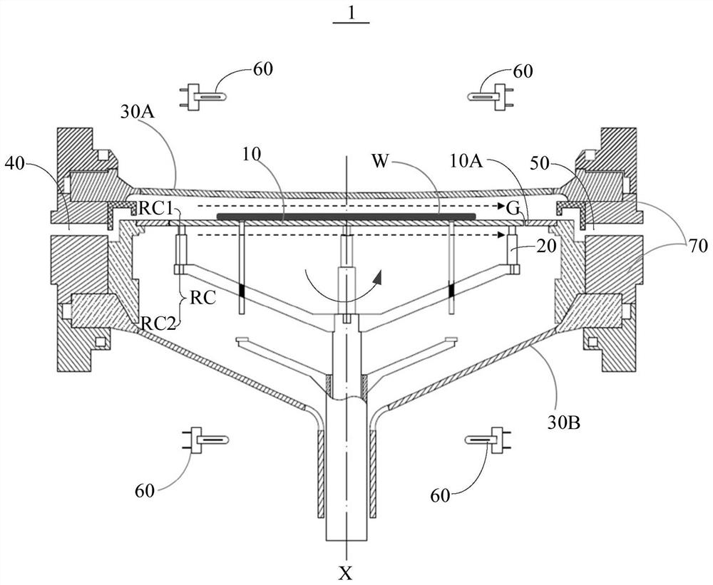
[0038] see image 3 , which shows a schematic diagram of an existing device 1 for epitaxial growth of a silicon wafer W. Such as image 3 As shown, the device 1 may include: a base 10, which is used to carry a silicon wafer W; a base support frame 20, which is used to support the base 10 and drive the base during epitaxial growth. 10 rotates around the central axis X at a certain speed, wherein during the rotation of the base 10, the silicon wafer W rotates around the central axis X together with the base 10, that is to say, the silicon wafer W remains stationary relative to the base 10, Thus, a small gap G is required between the radial edge of the susceptor 10 and the adjacent part 10A (typically the preheating ring); the upper quartz bell 30A and the lower quartz bell 30B...


PUM

PropertyMeasurementUnit
lengthaaaaaaaaaa

Abstract

The embodiment of the invention discloses a base supporting frame, a device and a method for epitaxial growth of a silicon wafer. The base supporting frame comprises: four base supporting arms, which extend outwards in a radial direction and extend upwards in an axial direction from the longitudinal axis of the base supporting frame, wherein the four base supporting arms are evenly distributed in a circumferential direction around the longitudinal axis, and the far end parts of the four base supporting arms support a base used for bearing the silicon wafer together; and four concave lenses, which are respectively connected to the four base supporting arms, wherein each concave lens extends along the connected base supporting arm, the four concave lenses are arranged in a manner that four <110> crystal orientations corresponding to the silicon wafer borne in the base are respectively aligned with the four base supporting arms in a vertical direction, and radiant heat radiated to four <110> crystal orientation positions of the silicon wafer through the four concave lenses in a vertical direction can be refracted and diffused by the four concave lenses.

Description

technical field [0001] Embodiments of the present invention relate to the technical field of epitaxial growth of silicon wafers, and in particular to a base supporting frame, device and method for epitaxial growth of silicon wafers. Background technique [0002] The epitaxial growth process of silicon wafers is an important process in the semiconductor chip manufacturing process. This process refers to growing a layer of crystal-free primary particles (Crystal Originated Particles, COP) defect and oxygen-free precipitated silicon single crystal layer. Epitaxial growth of silicon wafers mainly includes growth methods such as vacuum epitaxial deposition, vapor phase epitaxial deposition, and liquid phase epitaxial deposition, among which vapor phase epitaxial deposition is the most widely used. If not otherwise stated, the epitaxial growth mentioned in the present invention refers to the epitaxial growth accomplished by vapor phase epitaxial deposition. [0003] For the epit...

Claims


Application Information

Patent Timeline
Patent Type & Authority Applications(China)
IPC IPC(8): C30B23/02C30B25/12C30B29/06
CPCC30B23/02C30B25/12C30B29/06Y02P70/50
Inventor 俎世琦金柱炫
Owner XIAN ESWIN MATERIAL TECH CO LTD
Why Eureka
Try Eureka