Shielding substrate, circuit board and manufacturing method of shielding substrate and circuit board

A production method and circuit board technology, which is applied in the production of circuit boards, shielding substrates and circuit boards, and in the field of shielding substrates, can solve the problems of multi-layer single-sided board warping and inability to attach parts, etc.

Pending Publication Date: 2021-11-05
SHENZHEN KINWONG ELECTRONICS
View PDF4 Cites 0 Cited by
  • Summary
  • Abstract
  • Description
  • Claims
  • Application Information

AI Technical Summary

Problems solved by technology

[0004] However, when the finished boards in the related art are subjected to reflow soldering, it is easy to cause warping of the multi-layer board and / or single sided board, resulting in the failure to mount the parts.

Method used


Image

  • Shielding substrate, circuit board and manufacturing method of shielding substrate and circuit board
  • Shielding substrate, circuit board and manufacturing method of shielding substrate and circuit board
  • Shielding substrate, circuit board and manufacturing method of shielding substrate and circuit board

Examples


Embodiment Construction

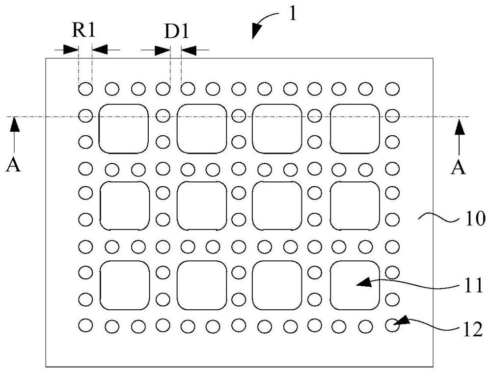
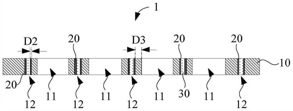
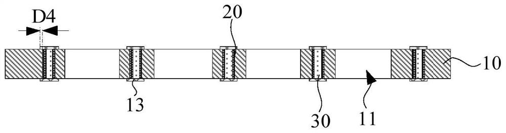
[0067] In order to make the purposes, technical solutions and advantages of the embodiments of the present application clearer, the technical solutions in the embodiments of the present application will be clearly and completely described below in conjunction with the drawings in the embodiments of the present application. Obviously, the described embodiments It is a part of the embodiments of this application, not all of them. Based on the embodiments in this application, all other embodiments obtained by persons of ordinary skill in the art without creative efforts fall within the protection scope of this application.

[0068] In the description of the embodiments of the present application, the terms "first" and "second" are used for description purposes only, and cannot be understood as indicating or implying relative importance or implicitly indicating the quantity of indicated technical features. Thus, the features defined as "first" and "second" may explicitly or implic...


PUM

PropertyMeasurementUnit
Thicknessaaaaaaaaaa
Apertureaaaaaaaaaa

Abstract

The invention provides a shielding substrate, a circuit board and a manufacturing method of the shielding substrate and the circuit board. The shielding substrate comprises a substrate body, wherein a plurality of shielding cavities are formed in the substrate body, the shielding cavities penetrate through the two opposite surfaces of the substrate body, and the substrate body is made of a non-metal material; and a metal shielding layer which is arranged on the periphery of each shielding cavity in a surrounding manner. According to the shielding substrate, the circuit board and the manufacturing method of the shielding substrate and the circuit board provided by the invention, the condition of warping of the finished circuit board during reflow soldering pasting can be avoided, and smooth pasting can be ensured; and in addition, the processing cost of the shielding substrate can be reduced.

Description

technical field [0001] The present application relates to the technical field of communications, and in particular to a shielding substrate, a circuit board, and a method for manufacturing the shielding substrate and the circuit board. Background technique [0002] With the development of communication technology, low-orbit satellite communication Internet technology that can achieve global coverage will make the Internet of Everything a reality. Low-orbit satellite communication must realize the transmission, transmission and reception of signals between satellites, ground receiving stations and end users. To ensure the stability and integrity of signal transmission, it is usually necessary to use a radar antenna. At present, the phased array radar antenna PCB that integrates radar antenna functions and ordinary multilayer printed circuit boards (Printed Circuit Board, PCB) is a low-orbit satellite satellite. In the chain system, it is an important part of signal transmissi...

Claims


Application Information

Patent Timeline
IPC IPC(8): H05K1/03H05K1/02H05K1/14H05K3/00H05K3/42H05K3/46
CPCH05K1/0326H05K1/0216H05K1/144H05K3/0044H05K3/42H05K3/4611
Inventor 白亚旭熊星宇曾浩王俊
Owner SHENZHEN KINWONG ELECTRONICS
Why Eureka
Try Eureka