
Method for optimizing via hole anti-pad wiring, circuit board, equipment and storage medium

A technology of anti-pad and printed circuit board, which is applied in the direction of printed circuit, printed circuit manufacturing, printed circuit components, etc., can solve the problems of complex board manufacturing process, failure to meet design requirements, increase cost, etc., to improve the chain The continuity of road impedance, the optimization of via impedance, and the effect of reducing signal reflection

Active Publication Date: 2021-11-05
LANGCHAO ELECTRONIC INFORMATION IND CO LTD
View PDF4 Cites 3 Cited by
  • Summary
  • Abstract
  • Description
  • Claims
  • Application Information

AI Technical Summary

Problems solved by technology

Although this design method can change the impedance at the via hole and reduce the impedance discontinuity, due to the different length of the via hole and the length of the stump, the size of the anti-pad is also different, which makes the board manufacturing process complicated. increase cost
On the other hand, for ultra-high-speed vias with back drilling, the design requirements may still not be met only through anti-pad optimization, which makes the above method limited

Method used


Image

  • Method for optimizing via hole anti-pad wiring, circuit board, equipment and storage medium
  • Method for optimizing via hole anti-pad wiring, circuit board, equipment and storage medium
  • Method for optimizing via hole anti-pad wiring, circuit board, equipment and storage medium

Examples


Embodiment 1

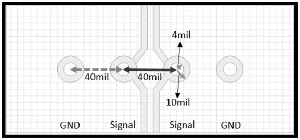
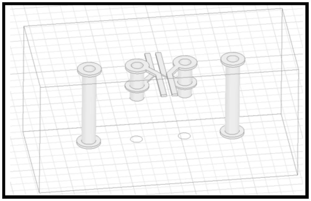
[0036] In order to further illustrate the design method of the present invention, a specific via is taken as an example to describe in detail, as figure 1 The via design of a PCIe Gen4 link is given, in which the radius of the signal hole is 4mil, and the radius of the via pad (via pad) is 10mil. The signal traces on the via hole are changed from layer L1 to layer L5. Such as figure 2 A three-dimensional diagram of the via design of a PCIe Gen4 link in China is given. The target controlled impedance of the vias is 85ohm±2ohm.

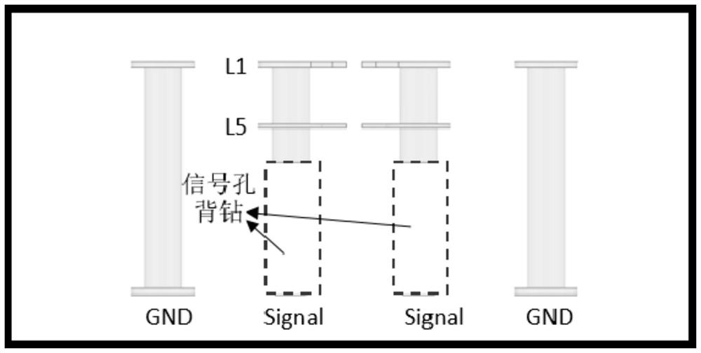
[0037]Due to the high signal rate, the via hole has a 51mil via stub (via stub), so the signal hole is back-drilled, and the back-drilling depth is 41mil, such as image 3 The back-drilling of the vias is given, and only the back-drilling is performed for the signal holes. Figure 4 It shows the Antipad design situation of the via hole, set the Antipad radius as the variable Antipad, take 15mil as the initial value, and use 5mil as the step size to...

Embodiment 2

[0084] Based on the method for optimizing via anti-pad wiring provided in Embodiment 1 of the present invention, Embodiment 2 of the present invention proposes a printed circuit board. The printed circuit board is processed by optimizing the routing of the anti-pad of the via hole; the method of making the printed circuit board is: for the anti-pad of the via hole of different sizes, the first value of the first distance is used as the initial value, and the second The numerical value is the step size for traversal, and the first distance corresponding to the minimum impedance of the via is determined; the first distance is the straight-line distance between the differential line coupling position in the anti-pad of the via and the middle of the differential signal hole.

[0085] The first value is 0mil or the radius of the via anti-pad. When the first value is 0mil, the second value is any value greater than 0 and less than the radius of the via anti-pad; when the first value...

Embodiment 3

[0098] Based on the method for optimizing via anti-pad routing proposed in Embodiment 1 of the present invention, Embodiment 3 of the present invention proposes a via-anti-pad routing optimization device for printed circuit boards, including:

[0099] The memory is used for storing the computer program; the processor is used for implementing the method steps of optimizing the routing of the via hole anti-pad when executing the computer program. The process of the method is:

[0100] For via anti-pads of different sizes, the first value of the first distance is used as the initial value, and the second value is used as the step size to traverse to determine the first distance corresponding to the minimum via hole impedance; the first distance is the over The linear distance between the differential line coupling position in the anti-pad of the hole and the middle of the differential signal hole.

[0101] The first value is 0mil or the radius of the via anti-pad. When the firs...


PUM


Abstract

The invention provides a method for optimizing via hole anti-pad wiring, a circuit board, equipment and a storage medium. The method comprises the following steps: aiming at via hole anti-bonding pads with different sizes, performing traversal by taking a first numerical value of a first distance as an initial value and a second numerical value as a step length, and determining the corresponding first distance when the via hole impedance is minimum, wherein the first distance is the linear distance between the coupling position of the differential line in the via hole anti-bonding pad and the middle of the differential signal hole; when the routing mode in the anti-pad area is optimized, carrying out the back drilling on the signal holes in the anti-pad area. Based on the method, the invention further provides a printed circuit board, via hole anti-pad routing optimization equipment of the printed circuit board and a storage medium. According to the invention, the impedance characteristic of the via hole needs to be concerned when the high-speed link is designed, and when the impedance of the via hole is optimized, besides changing the size of the anti-pad, the wiring mode in the anti-pad area can be optimized, so that the impedance of the via hole is further optimized, the impedance continuity of the link is improved, and the signal transmission quality is improved.

Description

technical field [0001] The invention belongs to the technical field of printed circuit board design, and in particular relates to a method, a circuit board, a device and a storage medium for optimizing the routing of via hole anti-pads. Background technique [0002] With the rapid development of microelectronics technology, the rising edge of the signal is getting faster and faster, and the transmission line effect produced by high-speed circuits is becoming more and more serious. For the current mainstream high-speed circuits, PCB engineers must adopt high-speed PCB design technology based on transmission line theory to ensure the normal operation of the circuit. The design and control of characteristic impedance is the core and foundation to solve the transmission line effect of high-speed circuits, and it has been paid more and more attention by PCB engineers and manufacturers. In order to obtain the final high-precision characteristic impedance circuit board products, i...

Claims


Application Information

Patent Timeline
Patent Type & Authority Applications(China)
IPC IPC(8): H05K3/00H05K1/02
CPCH05K3/00H05K3/0044H05K1/02
Inventor 荣世立
Owner LANGCHAO ELECTRONIC INFORMATION IND CO LTD
Learn More