Laminated packaging structure for mounting multiple circuit boards

A stacked packaging, multi-circuit technology, applied in the structural connection of printed circuits, printed circuits, and support structure installation, etc., can solve the problems of difficult protection, easy damage to the circuit board, affecting the working efficiency of the chip, etc., to reduce the occupied space, strong Thermal conductivity, the effect of convenient heat dissipation

Active Publication Date: 2021-11-09
江苏汉瑞通信科技有限公司
View PDF5 Cites 2 Cited by
  • Summary
  • Abstract
  • Description
  • Claims
  • Application Information

AI Technical Summary

Problems solved by technology

[0003] Existing printed circuit boards, with the high integration of smart devices, the power is getting bigger and bigger, and the heat dissipation of the circuit board has become a problem that must be considered in the packaging process, especially for complex smart devices that tend to be in a small space Install multiple circuit boards, the heat generated by the circuit board itself, except for a small part of the heat dissipated through the bottom carrier board and solder joints, the main heat is through natural heat dissipation, but if multiple circuit boards ar

Method used


Image

  • Laminated packaging structure for mounting multiple circuit boards
  • Laminated packaging structure for mounting multiple circuit boards
  • Laminated packaging structure for mounting multiple circuit boards

Examples


Embodiment

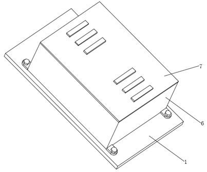
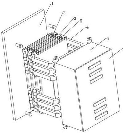
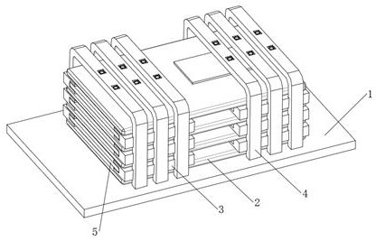
[0042] see Figure 1-6, a stacked packaging structure for multi-circuit board installation, including a mounting board 1, a plurality of evenly distributed printed circuit board bodies 2 are arranged on the mounting board 1, and a heat conducting plate 201 is fixedly connected to the bottom end of the printed circuit board body 2 , the heat conduction plate 201 is laid with a heat conduction film, and the printed circuit board main body 2 is provided with a plurality of pairs of positioning mounting holes matching the buffer shelf plate 3, so that the printed circuit board main body is clamped on the buffer shelf plate 3 through the heat conduction plate. Two pairs of buffer frame plates 3 are connected between two adjacent printed circuit board main bodies 2. The buffer frame plates 3 include an L-shaped frame plate 301. A buffer belt 5 and a hollow bag tube 501 are connected between a pair of L-shaped frame plates 301. The inner wall of the inner wall is fixedly connected wi...


PUM


Abstract

The invention discloses a laminated packaging structure for mounting multiple circuit boards, and belongs to the field of printed circuit boards. The laminated packaging structure for mounting the multiple circuit boards comprises a mounting plate, a plurality of uniformly distributed printed circuit board bodies are arranged on the mounting plate, two pairs of buffer frame plates are connected between every two adjacent printed circuit board bodies. Each buffer frame plate comprises L-shaped frame plates, a buffer strip is connected between the pair of L-shaped frame plates, and a supporting plate matched with the buffer strip is connected to the L-shaped frame plates in a sliding mode. The bottom end of the printed circuit board body is fixedly connected with the supporting plates, and a plurality of guide pipes matched with the buffer strip are fixedly connected to the L-shaped frame plates. A series connection frame comprises a plurality of segment columns. An arc-shaped frame is connected between the two segment columns at the top end. Therefore, a plurality of circuit boards can be mounted in a laminated manner, the occupied space of the circuit boards on a plane is reduced, the circuit boards can be effectively and comprehensively protected after the circuit boards are mounted in the laminated manner, and meanwhile, the heat dissipation of the circuit boards is facilitated.

Description

technical field [0001] The invention relates to the field of printed circuit boards, in particular to a stacked package structure for mounting multiple circuit boards. Background technique [0002] With the rapid development of wireless communication, automotive electronics and other consumer electronics, microelectronic packaging technology is developing in the direction of multi-function, miniaturization, portability, high speed, low power consumption and high reliability. Among them, system-in-package is a new type of packaging technology, which can effectively reduce the packaging area. [0003] Existing printed circuit boards, with the high integration of smart devices, the power is getting bigger and bigger, and the heat dissipation of the circuit board has become a problem that must be considered in the packaging process, especially for complex smart devices that tend to be in a small space Install multiple circuit boards, the heat generated by the circuit board itse...

Claims


Application Information

Patent Timeline
IPC IPC(8): H05K7/14H05K7/20H05K1/14
CPCH05K7/1404H05K7/2039H05K7/205H05K7/20509H05K7/20136H05K1/144
Inventor 王妙双
Owner 江苏汉瑞通信科技有限公司
Why Eureka
Try Eureka