
Photosensitive resin composition, photosensitive resin film, multilayer printed wiring board, semiconductor package, and method for producing multilayer printed wiring board

A photosensitive resin and composition technology, applied in the field of photosensitive resin compositions, can solve the problems of reduced photosensitive properties such as sensitivity and resolution of the photosensitive layer, insufficient peelability, and difficulty in taking into account the peelability of the support film and the photosensitivity performance. , to achieve the effect of efficient manufacturing and excellent peelability

Pending Publication Date: 2021-11-09
RESONAC CORPORATION
View PDF4 Cites 0 Cited by
  • Summary
  • Abstract
  • Description
  • Claims
  • Application Information

AI Technical Summary

Problems solved by technology

By adding a release agent, the detachability of the photosensitive layer and the support film can indeed be improved, but this method is difficult to balance the detachability and photosensitive performance of the support film.
Specifically, it is known that if the addition amount of the release agent in the photosensitive layer is small, the release property from the support film will become insufficient. On the other hand, if the addition amount of the release agent is increased, the photosensitive layer will Sensitivity and resolution and other photosensitive properties tend to decrease (for example, refer to paragraph [0010] of Patent Document 4), so it is urgently desired to develop a photosensitive resin composition that has both photosensitive properties and peelability from the support film.

Method used


Image

  • Photosensitive resin composition, photosensitive resin film, multilayer printed wiring board, semiconductor package, and method for producing multilayer printed wiring board
  • Photosensitive resin composition, photosensitive resin film, multilayer printed wiring board, semiconductor package, and method for producing multilayer printed wiring board
  • Photosensitive resin composition, photosensitive resin film, multilayer printed wiring board, semiconductor package, and method for producing multilayer printed wiring board

Examples


Embodiment

[0375] Hereinafter, although an Example demonstrates this invention in detail, this invention is not limited to these Examples.

[0376] In addition, the photosensitive resin composition obtained in each example evaluated the characteristic by the method shown below.

[0377] [1. Evaluation of photosensitive characteristics (through-hole resolution)]

[0378] On a copper-clad laminate substrate (MCL-E-67, manufactured by Hitachi Chemical Co., Ltd.) with a thickness of 1.0 mm, the protective film (protective layer) of the photosensitive resin film with the support film and protective film produced in each example was ) was peeled off, and a laminated body having a photosensitive layer was obtained by performing a lamination process using a pressure-type vacuum laminator (MVLP-500, manufactured by Meiki Seisakusho Co., Ltd., model number). It should be noted that the lamination conditions were set as follows: crimping pressure 0.4 MPa, pressure heating plate temperature 75° C.,...

Synthetic example 1

[0388] Synthesis of acid-modified epoxy derivative 1 [(A1-1) component] containing ethylenically unsaturated group and alicyclic skeleton

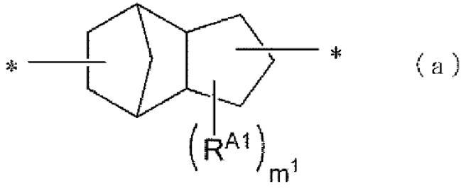
[0389] Add dicyclopentadiene type epoxy resin [Nippon Kayaku Co., Ltd. "XD-1000", epoxy equivalent 252g / eq, softening point 74.2 ° C, equivalent to (a1) component, by the above general formula (a1-1 )express. The number of ring-forming carbon atoms of the alicyclic skeleton: 10] 250 parts by mass, 70 parts by mass of acrylic acid (corresponding to component (a2)) 70 parts by mass, 0.5 parts by mass of methylhydroquinone, 120 parts by mass of carbitol acetate, heated Reaction was carried out at 90° C. with stirring, and the mixture was completely dissolved.

[0390] Next, the obtained solution was cooled to 60 degreeC, 2 mass parts of triphenylphosphine was added, it heated at 100 degreeC, and it reacted until the acid value of a solution became 1 mgKOH / g. 98 parts by mass of tetrahydrophthalic anhydride (corresponding to component (a3))...

Embodiment 1~6、 comparative example 1~4

[0393] (Preparation of photosensitive resin composition)

[0394] The composition was compounded according to the compounding composition and compounding quantity shown in Table 1, and it kneaded using the three-roll mill, and the photosensitive resin composition was prepared. In each example, methyl ethyl ketone was appropriately added to adjust the concentration, and a photosensitive resin composition having a solid content concentration of 60% by mass was obtained.

[0395] (Production of photosensitive resin film)

[0396] A polyethylene terephthalate film (G2-16, manufactured by Teijin Co., Ltd., trade name) with a thickness of 16 μm was used as a support film, and the photosensitive resin composition prepared in each example was prepared at a film thickness after drying. It coated on this support film so that it might become 5 micrometers, and dried at 75 degreeC for 30 minutes using the hot-air convection type dryer, and formed the photosensitive resin film (photosensi...


PUM

PropertyMeasurementUnit
acid valueaaaaaaaaaa
thicknessaaaaaaaaaa
particle diameteraaaaaaaaaa

Abstract

The present invention provides: a photosensitive resin composition which has both excellent photosensitive characteristics and excellent removability from a support film; a photosensitive resin composition for photo via formation; and a photosensitive resin composition for interlayer insulating layers. The present invention also provides: a photosensitive resin film and a photosensitive resin film for interlayer insulating layers, each of which is formed from the above-described photosensitive resin composition; a multilayer printed wiring board; a semiconductor package; and a method for producing the multilayer printed wiring board. The above-described photosensitive resin composition specifically contains (A) a photopolymerizable compound having an ethylenically unsaturated group, (B) a photopolymerization initiator and (C) a thermosetting resin; the photopolymerizable compound (A) having an ethylenically unsaturated group contains (A1) a photopolymerizable compound that has an acidic substituent and an alicyclic skeleton together with an ethylenically unsaturated group; the thermosetting resin (C) contains (C1) a thermosetting resin that has an alicyclic skeleton; and the content of component (C1) is 10 parts by mass or more relative to 100 parts by mass of component (A).

Description

technical field [0001] This indication relates to the manufacturing method of a photosensitive resin composition, a photosensitive resin film, a multilayer printed wiring board, a semiconductor package, and a multilayer printed wiring board. Background technique [0002] In recent years, the miniaturization and high performance of electronic equipment have been promoted, and the density of multilayer printed wiring boards is increasing due to the increase in the number of circuit layers and the miniaturization of wiring. In particular, the density of semiconductor packaging substrates such as BGA (ball grid array) and CSP (chip size package) on which semiconductor chips are mounted is significantly higher, and in addition to the miniaturization of wiring, the insulation film Thin film and further reduction in diameter of via holes for interlayer connection (also called "via holes"). [0003] As a method of manufacturing a printed wiring board, a method of manufacturing a mu...

Claims


Application Information

Patent Timeline
Patent Type & Authority Applications(China)
IPC IPC(8): G03F7/004G03F7/027H05K1/03H05K3/46
CPCG03F7/027G03F7/038H05K1/0373H05K3/4676H05K3/4661H05K2201/0209G03F7/004G03F7/028G03F7/032H05K1/03H05K3/46H01L21/4857H01L23/49822H01L23/49894H05K1/0326
Inventor 泽本飒人中村彰宏高濑有司野本周司冈出翔太
Owner RESONAC CORPORATION
Learn More