Self-bias photoelectric detector and preparation method and application thereof

A photodetector and self-bias technology, which is applied in the field of photodetectors, can solve the problems of low photodetector responsivity, low photocurrent intensity, and self-bias photodetectors do not have photocurrent gain. High light extraction efficiency, good photosensitive characteristics, and the effect of improving the photoelectric response effect

Pending Publication Date: 2022-07-01
PEKING UNIV SHENZHEN GRADUATE SCHOOL
View PDF0 Cites 0 Cited by
  • Summary
  • Abstract
  • Description
  • Claims
  • Application Information

AI Technical Summary

Problems solved by technology

Self-biased detectors are highly sensitive, but self-biased photodetectors do not have photocurrent gain
Therefore, the responsivity of most existing self-powered photodetectors is not high, that is, the photocurrent intensity is not high under the same light intensity.

Method used


Image

  • Self-bias photoelectric detector and preparation method and application thereof
  • Self-bias photoelectric detector and preparation method and application thereof
  • Self-bias photoelectric detector and preparation method and application thereof

Examples


Embodiment

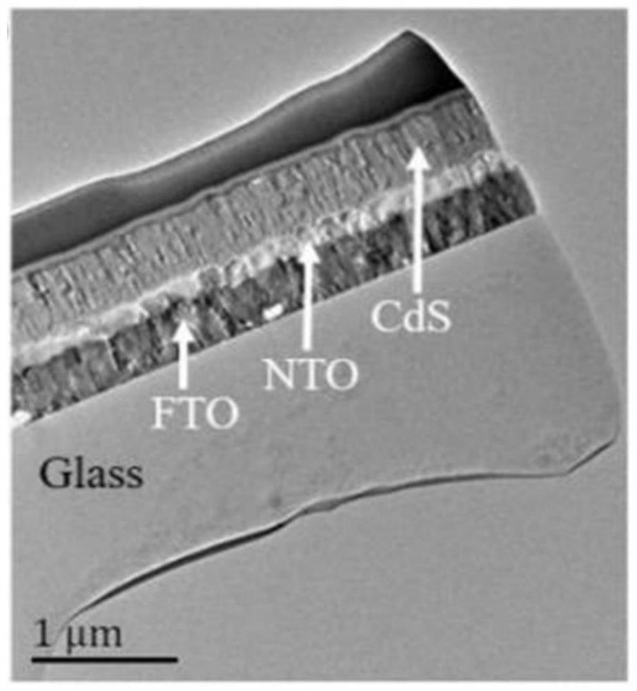
[0029] In the self-biased photodetector of this example, the substrate is FTO conductive glass. Niobium-doped titanium oxide film and CdS film are prepared by sputtering on the FTO conductive glass. Finally, silver paste is printed as the electrode to make the self-biased photodetector of this example. Piezoelectric photodetectors. The specific preparation method is as follows:

[0030] 1. Immerse the FTO conductive glass with acetone, alcohol and deionized water in sequence, and then perform ultrasonic cleaning on the soaked FTO conductive glass.

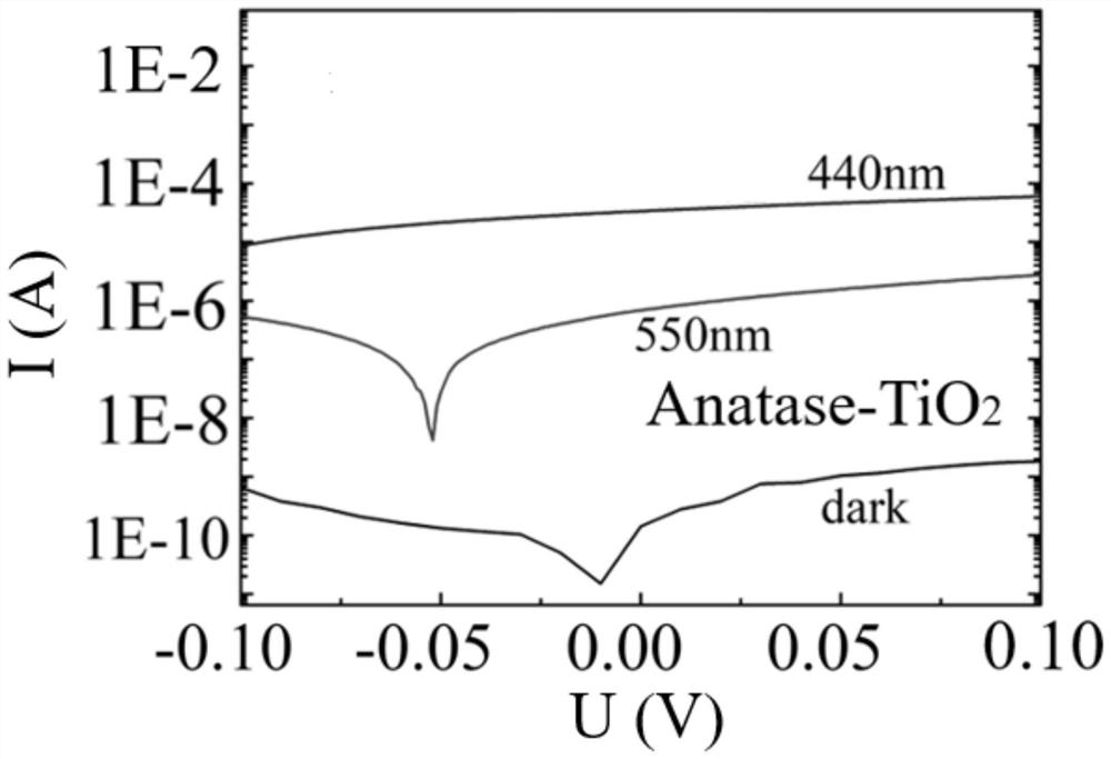
[0031] 2. Niobium-doped titanium oxide films were prepared on FTO conductive glass by vacuum sputtering method, where the pressure of the sputtering chamber was 0.3Pa, the atmosphere of the sputtering chamber was argon, the substrate temperature was 25°C, and the sputtering power was 5W , the deposition rate is 10 nm / min, and the sputtering time is 30 minutes to prepare a niobium-doped titanium dioxide film with a thickness of 300...


PUM

PropertyMeasurementUnit
thicknessaaaaaaaaaa

Abstract

The invention discloses a self-bias photoelectric detector and a preparation method and application thereof. The self-bias photoelectric detector comprises a substrate and a photoelectric structure fixed on the substrate, and the photoelectric structure comprises a photosensitive semiconductor layer, a blocking semiconductor layer and a counter electrode thin film layer. The photosensitive semiconductor layer is an n-type semiconductor material layer formed by cadmium sulfide; the barrier semiconductor layer is an n-type semiconductor material layer formed by titanium dioxide and/or metal-doped titanium dioxide. According to the self-bias photoelectric detector, cadmium sulfide is adopted as the photosensitive semiconductor layer, titanium dioxide and/or metal-doped titanium dioxide are/is adopted as the blocking semiconductor layer, the CdS layer has good photosensitive characteristics, and the CdS layer is matched with titanium dioxide to form a semiconductor junction, so that the leakage current can be reduced, and the photoelectric response effect can be improved. The self-bias photoelectric detector has the advantages of high reliability, low forward working voltage and high light extraction efficiency.

Description

technical field [0001] The present application relates to the technical field of photodetectors, and in particular, to a self-biased photodetector and a preparation method and application thereof. Background technique [0002] Photodetectors are the key components of future optical chip technology and optoelectronic integration technology, which require photodetectors with sufficiently high responsivity and response speed. The transparency of the device and the entry of the response band into the ultraviolet can make the photodetector work in sunlight, and can also integrate the detector under the screen, integrate on the glass, or prepare a fully transparent photodetector. Self-powered detectors have the characteristics of energy saving, permanent operation, and easy integration, and have been extensively studied. DC-AC nanogenerators based on self-powered photodetectors have also recently attracted great interest. Self-biased detectors are highly sensitive, but self-bias...

Claims


Application Information

Patent Timeline
Patent Type & Authority Applications(China)
IPC IPC(8): H01L31/0296H01L31/032H01L31/109H01L31/18
CPCH01L31/109H01L31/18H01L31/032H01L31/0321H01L31/0296
Inventor 潘锋梁军林海
Owner PEKING UNIV SHENZHEN GRADUATE SCHOOL
Why Eureka
Try Eureka