A method for preparing polycrystalline lead selenide thin films based on oxygen ion beam assisted deposition

An assisted deposition, oxygen ion beam technology, applied in chemical instruments and methods, ion implantation plating, polycrystalline material growth, etc., can solve the problems of CMOS process compatibility, limit the integrated application of photosensitive arrays, etc., to reduce absorption defects, good Optoelectronic properties and surface properties, the effect of optimizing optoelectronic properties

Active Publication Date: 2017-11-14
NORTHWESTERN POLYTECHNICAL UNIV
View PDF8 Cites 0 Cited by
  • Summary
  • Abstract
  • Description
  • Claims
  • Application Information

AI Technical Summary

Problems solved by technology

The chemical deposition method is simple and easy, and the process is relatively mature, but it is not compatible with the CMOS process, which limits its application in the integration of photosensitive arrays

Method used


Image

  • A method for preparing polycrystalline lead selenide thin films based on oxygen ion beam assisted deposition
  • A method for preparing polycrystalline lead selenide thin films based on oxygen ion beam assisted deposition
  • A method for preparing polycrystalline lead selenide thin films based on oxygen ion beam assisted deposition

Examples


Embodiment 1

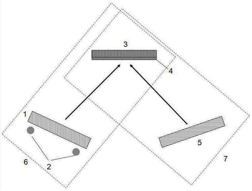
[0042] (1) The Si(100) substrate was ultrasonically cleaned for 15 min with absolute ethanol and acetone, and then washed with deionized water and dried for use. Si (100) substrate and PbSe powder (purity ≥ 99.99%) are respectively placed in the substrate frame 3 and the crucible 1 of the vacuum chamber, and the thermal evaporation system 6 is evacuated to 3 × 10 -4 Pa, and cover the substrate with a baffle. Increase the current of the heating source until the molecular beam evaporation rate reaches Reset the film thickness, remove the baffle, and start film growth with the substrate temperature stabilized at 120°C. When the thickness reaches 500nm, adjust the heating current to 0A and turn off the heating system to suspend the film growth. Start the ion source 5 to bombard the film with oxygen ions, the ion energy is 500eV, and the beam density is 100μA / cm 2 , the bombardment ends after 1 min. Use a baffle to block the film, and then increase the current of the heating s...

Embodiment 2

[0045] (1) The Si(100) substrate was ultrasonically cleaned for 15 min with absolute ethanol and acetone, and then washed with deionized water and dried for use. Si (100) substrate and PbSe powder (purity ≥ 99.99%) are respectively placed in the substrate frame 3 and the crucible 1 of the vacuum chamber, and the thermal evaporation system 6 is evacuated to 3 × 10 -4 Pa, and cover the substrate with a baffle. Increase the current of the heating source until the molecular beam evaporation rate reaches Reset the film thickness, remove the baffle, and start film growth with the substrate temperature stabilized at 120°C. When the film thickness reaches 1 μm, adjust the heating current to 0A and turn off the heating system to stop the film growth. Turn on the ion source 5, and the above-mentioned film is bombarded with oxygen ions, the ion energy is 500eV, and the beam current density is 100μA / cm 2 , the bombardment ends after 1 min.

[0046] (2) vacuum annealing is carried out...

Embodiment 3

[0048] (1) The Si(100) substrate was ultrasonically cleaned for 15 min with absolute ethanol and acetone, and then washed with deionized water and dried for use. Si (100) substrate and PbSe powder (purity ≥ 99.99%) are respectively placed in the substrate frame 3 and the crucible 1 of the vacuum chamber, and the thermal evaporation system 6 is evacuated to 3 × 10 -4 Pa, and cover the substrate with a baffle. Increase the current of the heating source until the molecular beam evaporation rate reaches Reset the film thickness, remove the baffle, and start film growth with the substrate temperature stabilized at 120°C. When the film thickness reaches 1 μm, adjust the heating current to 0A and turn off the heating system to stop the film growth. Turn on the ion source 5, and the above-mentioned film is bombarded with oxygen ions, the ion energy is 500eV, and the beam current density is 100μA / cm 2 , the bombardment ends after 1 min.

[0049] (2) The film obtained in the above ...


PUM

PropertyMeasurementUnit
thicknessaaaaaaaaaa
thicknessaaaaaaaaaa

Abstract

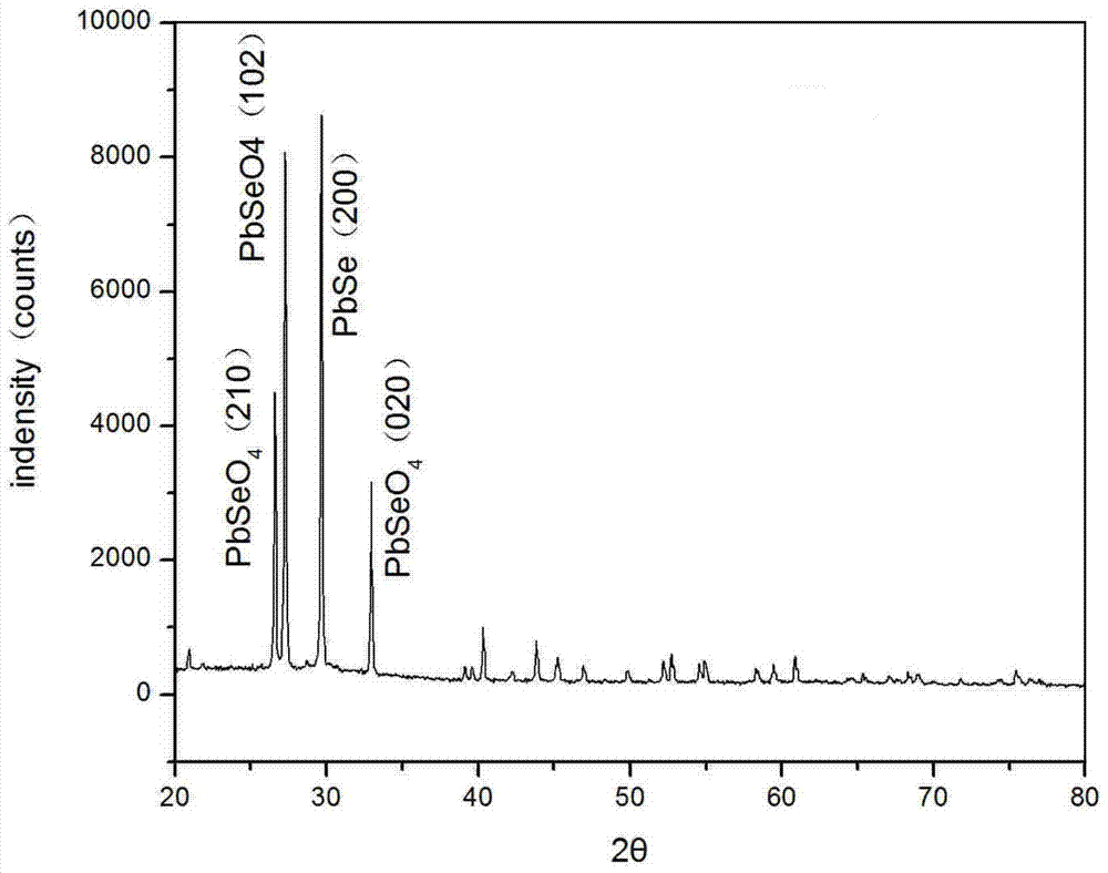
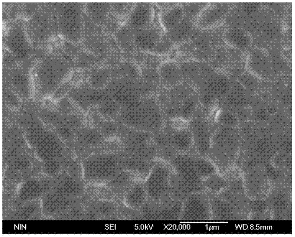
A method for preparing lead selenide polycrystalline thin films based on oxygen ion beam assisted deposition proposed by the present invention aims at the incorporation amount and depth of oxygen that cannot be accurately controlled in the PbSe thin film prepared by the current physical vapor deposition combined with atmosphere annealing method distribution problem, use ion beam assisted deposition technology, adopt static mixing method, carry out oxygen ion assisted bombardment on the surface after the film growth is completed, and then perform subsequent vacuum annealing on the film to prepare PbSe polycrystalline with good photosensitive properties and stability film. This method can precisely control the implantation dose and depth distribution of oxygen ions, and separates the oxygen doping from the polycrystallization process to increase the freedom of process optimization. The optical I-V characteristics, SEM, XRD and other preliminary characterizations of the prepared samples show that the PbSe polycrystalline thin film prepared by this method has good photoelectric properties and surface properties.

Description

technical field [0001] The invention belongs to the field of optoelectronic devices, relates to vacuum coating technology and infrared photoelectric detection technology, in particular to a method for preparing polycrystalline lead selenide thin film based on oxygen ion beam assisted deposition. Background technique [0002] Lead selenide (PbSe) is an important semiconductor material with a narrow bandgap (0.28eV). In recent years, uncooled mid-infrared detectors based on PbSe polycrystalline materials have attracted more and more attention. The detector can respond to mid-infrared radiation at room temperature, and has the advantages of fast response speed and high sensitivity. The detection device based on this technology can remove the refrigeration system and realize the miniaturization and portability design of the device. [0003] At present, the preparation of the material mainly adopts methods such as chemical synthesis and vapor deposition. The chemical deposition...

Claims


Application Information

Patent Timeline
Patent Type & Authority Patents(China)
IPC IPC(8): C30B28/12C30B29/46C23C14/06
Inventor 梅霆杨颢郑建邦陈磊刘旻张文定
Owner NORTHWESTERN POLYTECHNICAL UNIV
Why Eureka
Try Eureka