Method for making semiconductor device
A technology for semiconductors and devices, applied in the field of semiconductor devices and their manufacturing, can solve problems such as increasing the number of process steps
- Summary
- Abstract
- Description
- Claims
- Application Information
AI Technical Summary
Problems solved by technology
Method used
Image

Examples
Embodiment Construction
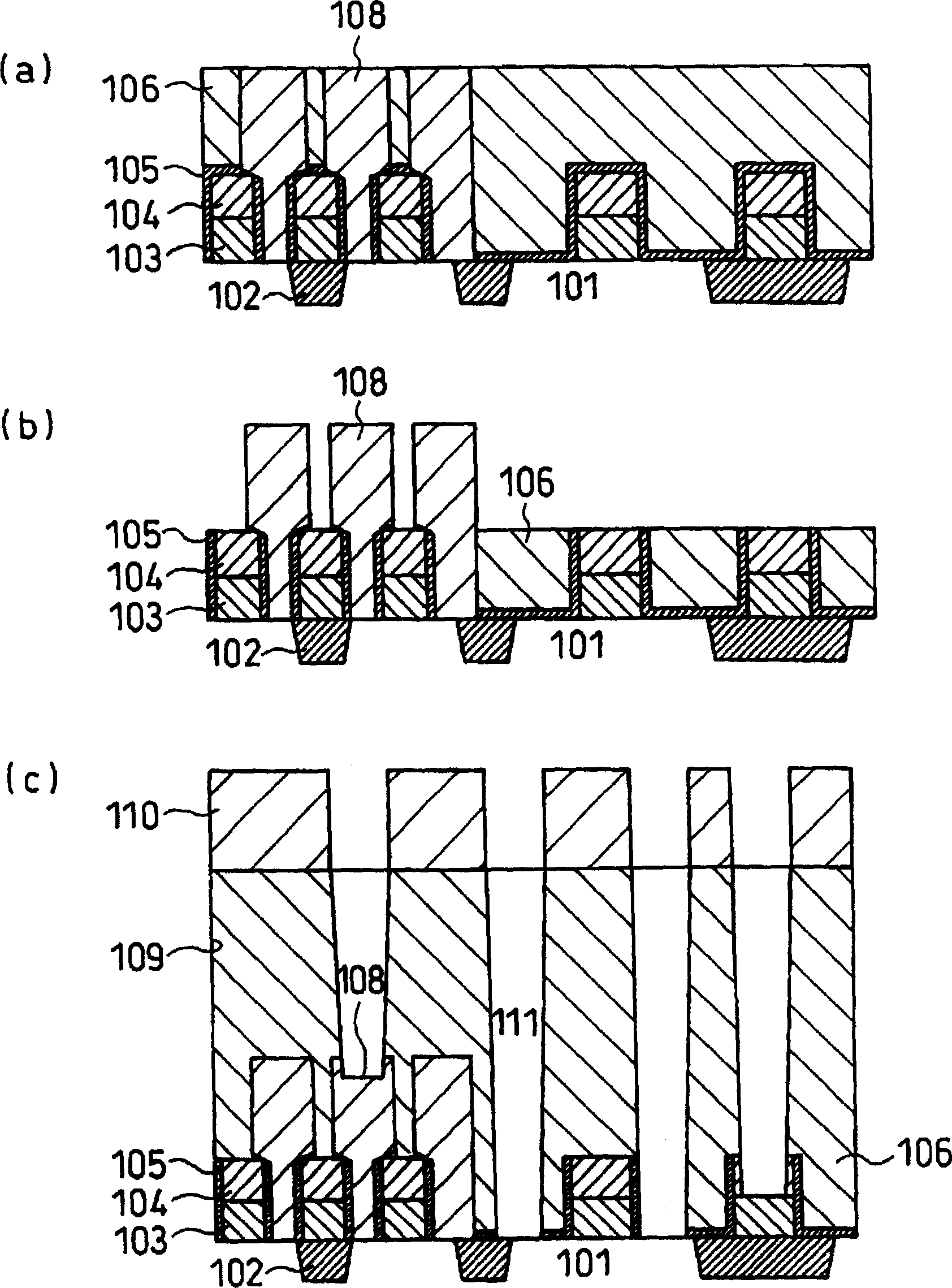
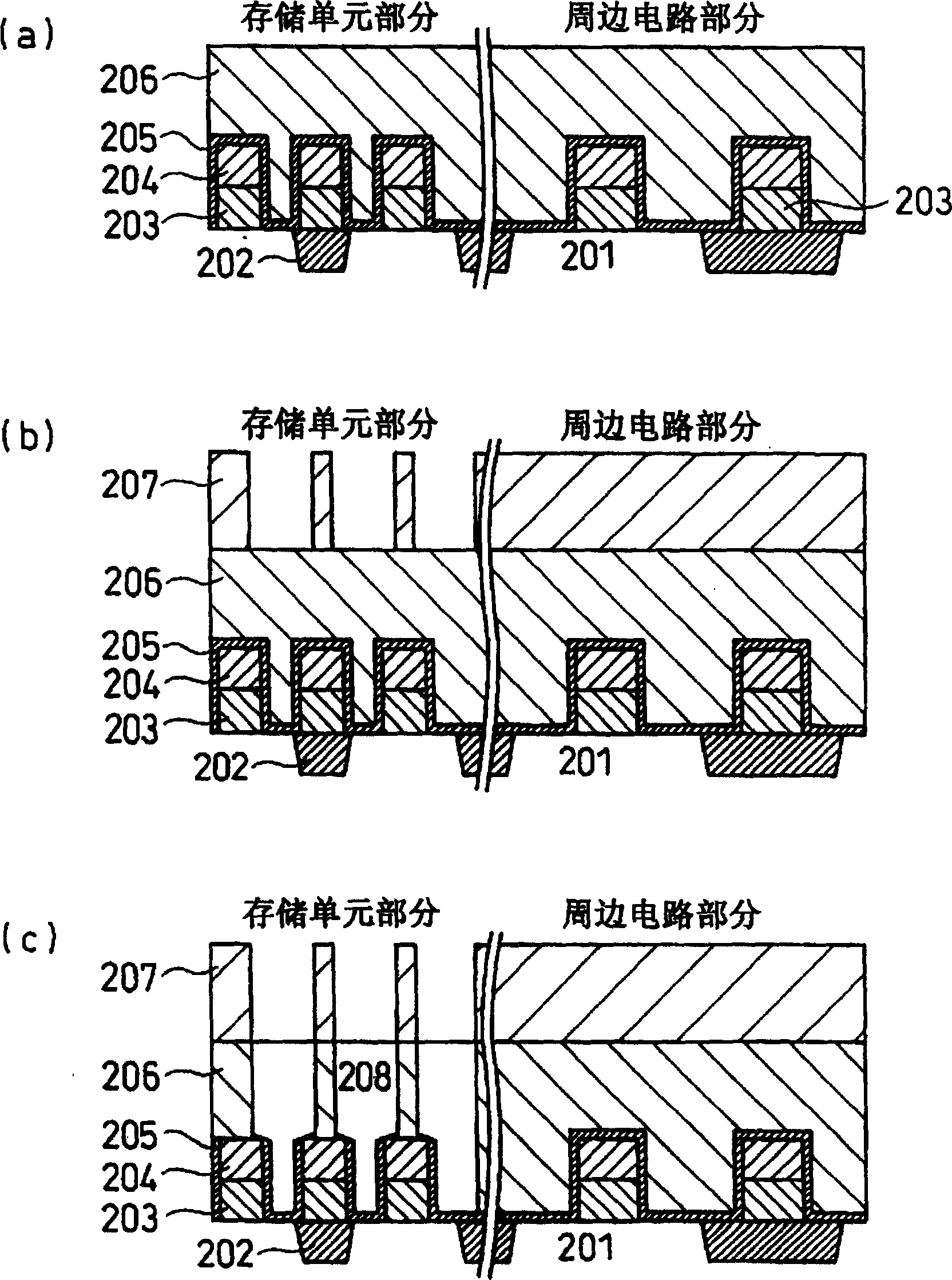
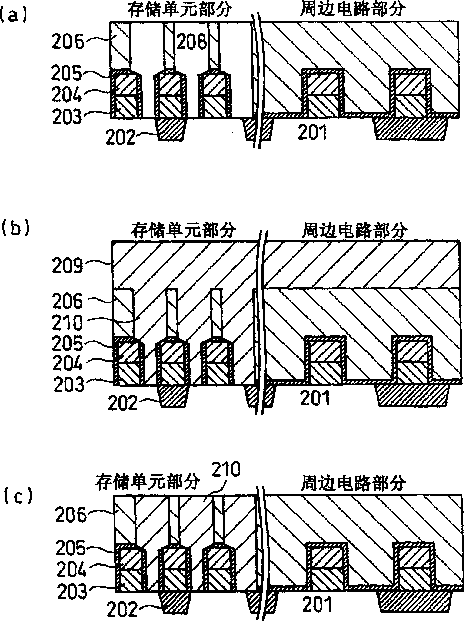
[0025] Hereinafter, an embodiment of a method for manufacturing a semiconductor device according to the present invention will be described in detail with reference to related drawings.
[0026] figure 2 Figure 6 A method of manufacturing a semiconductor device according to the present invention is shown.
[0027] In these drawings, figure 2 (a) represents a first step whereby a polysilicon film 203 and an insulating film 204 are formed on a semiconductor substrate 201, and then the polysilicon film 203 and the insulating film 204 are etched into a predetermined shape to form a gate electrode 203, and thereafter, the An etching stopper film 205 and an interlayer insulating film 206 are formed on the entire surface thereof.
[0028] figure 2 (c) represents a second step whereby a contact hole 208 reaching the semiconductor substrate is formed in the interlayer insulating film 206 so as to expose the etching stopper film 205 on the semiconductor substrate.
[0029] im...
PUM
 Abstract
Description
Claims
Application Information
 - R&D Engineer
- R&D Manager
- IP Professional
- Industry Leading Data Capabilities
- Powerful AI technology
- Patent DNA Extraction
Browse by: Latest US Patents, China's latest patents, Technical Efficacy Thesaurus, Application Domain, Technology Topic.
© 2024 PatSnap. All rights reserved.Legal|Privacy policy|Modern Slavery Act Transparency Statement|Sitemap