Substrate combining structure, substrate combining system and substrate combining method
A splicing system and substrate technology, applied in the structural connection of printed circuits, printed circuits, lithography/patterns, etc., can solve the problem that circuit boards cannot be spliced with circuit boards.
- Summary
- Abstract
- Description
- Claims
- Application Information
AI Technical Summary
Problems solved by technology
Method used
Image

Examples
no. 1 example
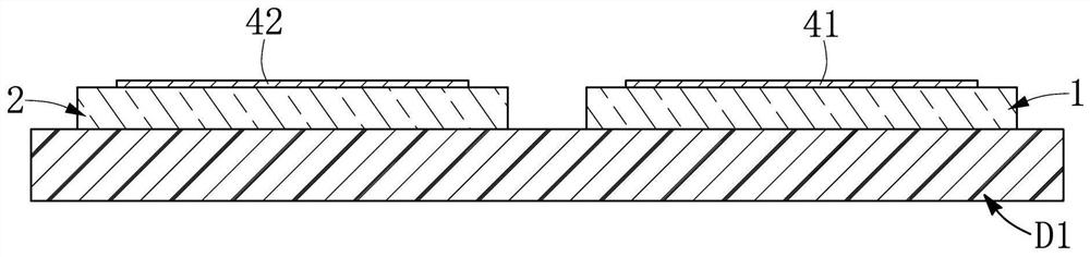
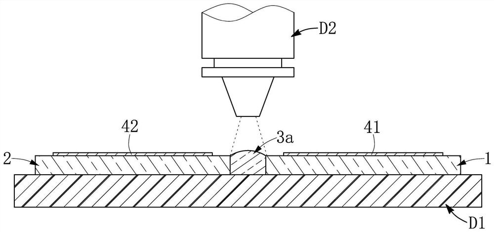
[0038] refer to Figure 1 to Figure 6 As shown, the first embodiment of the present invention provides a substrate splicing method, which includes: first, cooperate figure 1 and figure 2 As shown, a first circuit layer 41 and a second circuit layer 42 are respectively pre-disposed on a first glass substrate 1 and a second glass substrate 2 (step S100); then, cooperate figure 1 and figure 2 As shown, a substrate carrying device D1 is used to carry the first glass substrate 1 with the first circuit layer 41 and the second glass substrate 2 with the second circuit layer 42 (step S102); then, cooperate figure 1 and image 3 As shown, a connecting layer forming device D2 is used to form a glass connecting material 3a between the first glass substrate 1 and the second glass substrate 2 (step S104); figure 1 and Figure 4 As shown, through a material hardening device D3, to harden the glass connection material 3a (step S106); figure 1 , Figure 4 and Figure 5 As shown, a s...
no. 2 example
[0047] Cooperate Figure 7 As shown, the second embodiment of the present invention provides a substrate splicing structure S, which includes: a first glass substrate 1, a second glass substrate 2, a glass connecting material 3a (unprocessed glass connecting layer) and a Jumper wire W. Depend on Figure 7 and Figure 6It can be seen that the biggest difference between the second embodiment of the present invention and the first embodiment lies in: after finishing the production of the glass connecting material 3a (as in the first embodiment image 3 and Figure 4 As shown), the jumper circuit W provided by the second embodiment can be directly connected to the first circuit layer 41 and the Between the second circuit layer 42 .
no. 3 example
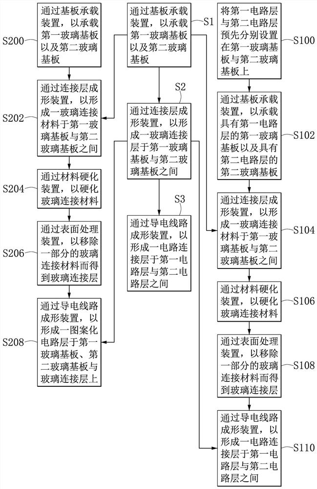
[0049] refer to figure 1 as well as Figure 8 to Figure 12 As shown, the second embodiment of the present invention provides a substrate splicing method, which includes: first, cooperate figure 1 and Figure 8 As shown, a substrate carrying device D1 is used to carry a first glass substrate 1 and a second glass substrate 2 (step S200); then, coordinate figure 1 and Figure 9 As shown, a connecting layer forming device D2 is used to form a glass connecting material 3a between the first glass substrate 1 and the second glass substrate 2 (step S202); then, cooperate figure 1 and Figure 10 As shown, through a material hardening device D3, to harden the glass connection material 3a (step S204); Next, cooperate figure 1 , Figure 10 and Figure 11 As shown, a surface treatment device D4 is used to remove a part of the glass connecting material 3a to obtain the glass connecting layer 3 (step S206); figure 1 and Figure 12 As shown, a patterned circuit layer 4 is formed on t...
PUM
 Abstract
Description
Claims
Application Information
 - R&D
- Intellectual Property
- Life Sciences
- Materials
- Tech Scout
- Unparalleled Data Quality
- Higher Quality Content
- 60% Fewer Hallucinations
Browse by: Latest US Patents, China's latest patents, Technical Efficacy Thesaurus, Application Domain, Technology Topic, Popular Technical Reports.
© 2025 PatSnap. All rights reserved.Legal|Privacy policy|Modern Slavery Act Transparency Statement|Sitemap|About US| Contact US: help@patsnap.com