Semiconductor high-voltage insulation test equipment

A high-voltage insulation and testing equipment technology, which is applied in the direction of electronic circuit testing, dielectric strength testing, optical testing flaws/defects, etc. It can solve the problems of increasing labor costs, inability to fully automate testing, and low testing efficiency, so as to reduce labor costs. , High test efficiency, avoiding the effect of accuracy

Active Publication Date: 2021-11-19
无锡昌鼎电子有限公司
View PDF11 Cites 3 Cited by
  • Summary
  • Abstract
  • Description
  • Claims
  • Application Information

AI Technical Summary

Problems solved by technology

[0003] The existing semiconductor high-voltage insulation test method is generally to manually place the chip in the test equipment, and then apply high-voltage electricity to the chip pins, and the test component detects whether there is leakage in the shell of the chip. Sorting, using this method, human error is likely to affect the accuracy of the test, and at the same time increases the labor cost, cannot fully automate the test, and the test efficiency is low

Method used


Image

  • Semiconductor high-voltage insulation test equipment
  • Semiconductor high-voltage insulation test equipment
  • Semiconductor high-voltage insulation test equipment

Examples


Embodiment Construction

[0036] The present invention will be described in detail below, and the technical solutions in the embodiments of the present invention will be clearly and completely described. Apparently, the described embodiments are only some of the embodiments of the present invention, not all of them. Based on the embodiments of the present invention, all other embodiments obtained by persons of ordinary skill in the art without making creative efforts belong to the protection scope of the present invention.

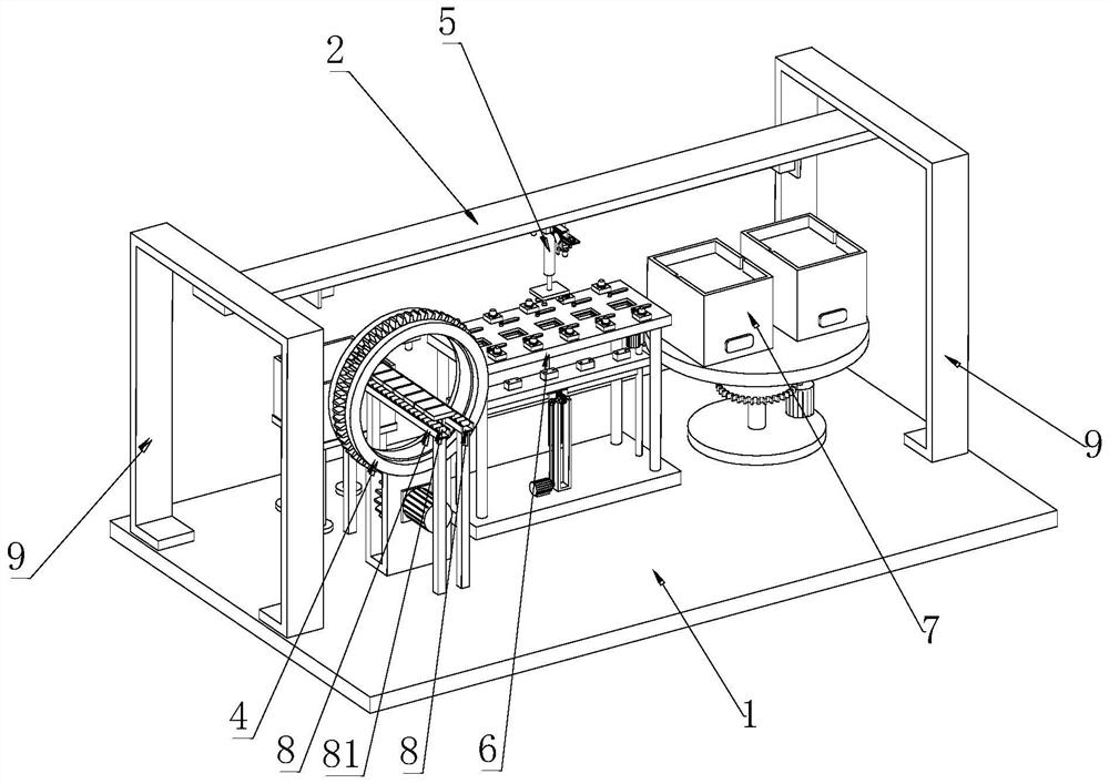
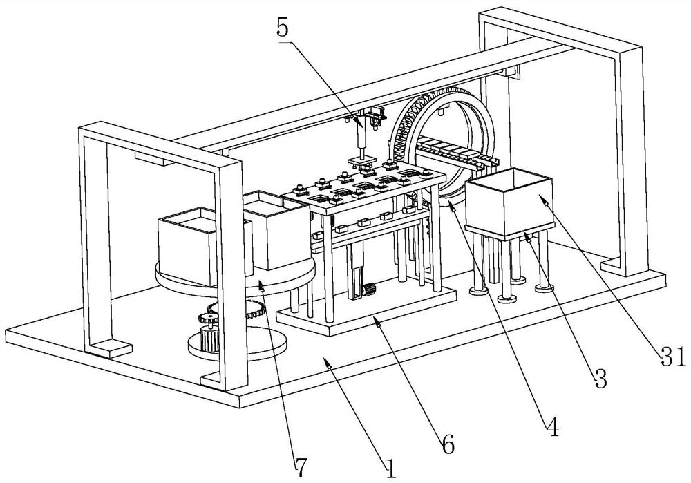
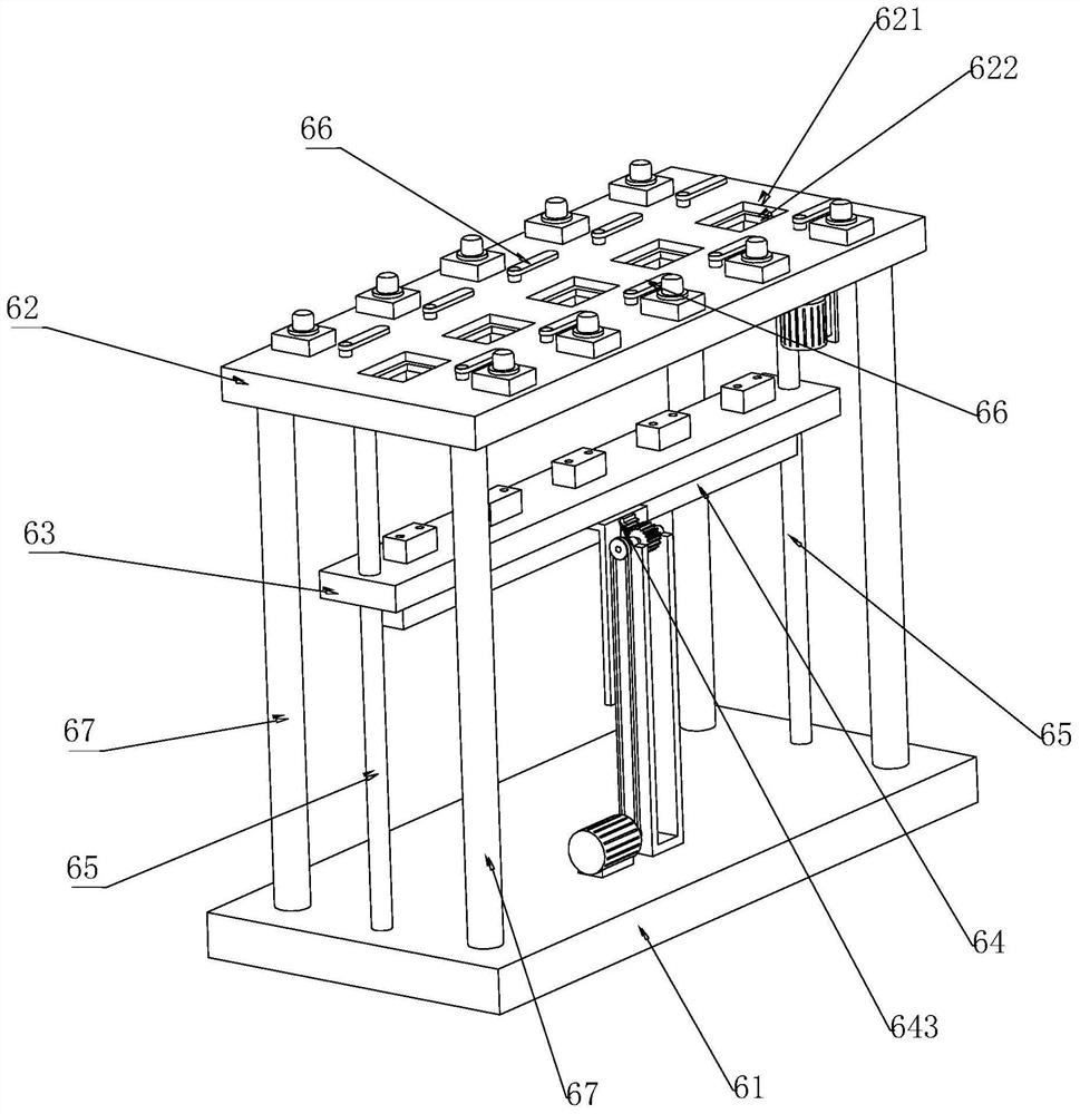
[0037] The present invention provides a kind of semiconductor high-voltage insulation test equipment here through improvement, as Figure 1-Figure 14 As shown, it includes a substrate 1, a horizontal plate 2, a support table 3, a waste bin 31, an appearance inspection component 4, a mobile sorting component 5, a high-voltage test component 6, a placement component 7, two chip transport racks 8 and two gantry frames 9. The two gantry frames 9 are arranged symmetrically on the top of...


PUM


Abstract

The invention relates to the technical field of semiconductor production, in particular to semiconductor high-voltage insulation test equipment. The equipment comprises a substrate, a transverse plate, a supporting table, a waste box, an appearance detection assembly, a movable sorting assembly, a high-voltage test assembly, a placement assembly, two chip conveying frames and two portal frames, the two portal frames are symmetrically arranged on the top of the substrate, the two sides of the transverse plate are connected with the top ends of the two portal frames correspondingly, the appearance detection assembly is arranged at the top of the substrate, the movable sorting assembly is installed at the bottom of the transverse plate, the high-voltage testing assembly is arranged between the two portal frames, and the placing assembly is arranged beside the high-voltage testing assembly. According to the invention, high-voltage testing operation is carried out on the chips in a full-automatic manner, the testing efficiency is high, the chips are classified and stored in a full-automatic manner according to the testing result of whether electric leakage occurs, the influence of human errors on the testing accuracy is avoided, and the labor cost is also reduced.

Description

technical field [0001] The invention relates to the technical field of semiconductor production, in particular to semiconductor high-voltage insulation testing equipment. Background technique [0002] A semiconductor refers to a material whose conductivity at room temperature is between that of a conductor and an insulator. Semiconductors are used in integrated circuits, consumer electronics, communication systems, photovoltaic power generation, lighting, high-power power conversion and other fields. For example, diodes are devices made of semiconductors. No matter from the perspective of technology or economic development, the importance of semiconductors is huge. The core units of most electronic products, such as computers, mobile phones or digital recorders, are closely related to semiconductors. Common semiconductor materials include silicon, germanium, gallium arsenide, etc., and silicon is the most influential one in the application of various semiconductor material...

Claims


Application Information

Patent Timeline
IPC IPC(8): G01R31/18G01R31/12G01R31/28G01N21/88G01N21/89
Inventor 陈能强
Owner 无锡昌鼎电子有限公司
Why Eureka
Try Eureka