Micro-strip plate and substrate welding device and using method

A welding device and microstrip board technology, applied in auxiliary devices, welding equipment, manufacturing tools, etc., can solve the problems of difficult welding void rate, high requirements for compact tooling, and inability to meet the welding efficiency of microwave circuit welding quality. Avoid warping or misalignment, and ensure the effect of reliability

Pending Publication Date: 2021-11-23
SHANGHAI RADIO EQUIP RES INST
View PDF8 Cites 0 Cited by
  • Summary
  • Abstract
  • Description
  • Claims
  • Application Information

AI Technical Summary

Problems solved by technology

However, with the development of science and technology, the signal frequency band used for microwave-based circuits is getting higher and higher, and the output scale is also getting larger and larger. When using traditional reflow soldering or artificial hot platform soldering technology for batch soldering of microstrip boards and substrates, It has been unable to meet the increasingly higher requirements of microwave circuits on welding quality (including void rate, penetration rate, thermal conductivity, etc.) and welding efficiency.
At present, the main reasons for restricting batch automatic welding of microstrip boards and substrates are as follows: 1. The positioning accuracy between microstrip boards and substrates is high, and the positioning accuracy is ≤±0.05mm; 2. The thickness of microstrip boards is relatively high. Thin (generally 0.254mm), high requirements on the press tooling; 3. The welding process needs to be uniform and continuous pressure on the microstrip board and the substrate to ensure that the microstrip board after welding will not warp due to thermal expansion Qu; 4. Welding void rate is difficult to solve by conventional equipment and conventional process methods

Method used


Image

  • Micro-strip plate and substrate welding device and using method
  • Micro-strip plate and substrate welding device and using method

Examples


Embodiment Construction

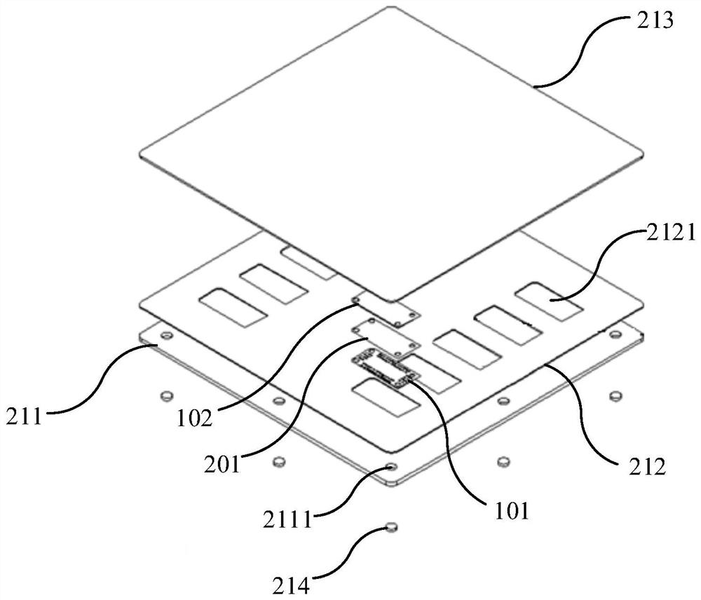
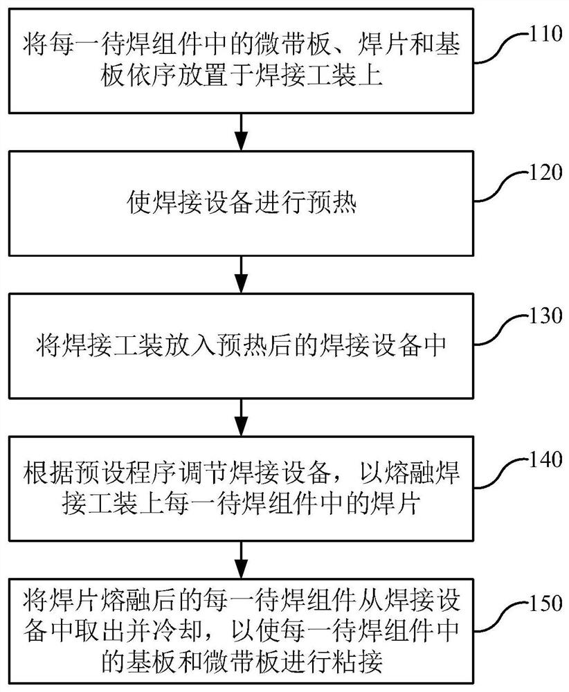
[0047]A microstrip plate and substrate welding device and its usage method proposed by the present invention will be further described in detail below in conjunction with the accompanying drawings and specific embodiments. The advantages and features of the present invention will become clearer from the following description. It should be noted that the drawings are in a very simplified form and all use imprecise scales, which are only used to facilitate and clearly assist the purpose of illustrating the embodiments of the present invention. In order to make the objects, features and advantages of the present invention more comprehensible, please refer to the accompanying drawings. It should be noted that the structures, proportions, sizes, etc. shown in the drawings attached to this specification are only used to match the content disclosed in the specification, for those who are familiar with this technology to understand and read, and are not used to limit the implementatio...


PUM


Abstract

The invention discloses a micro-strip plate and substrate welding device and a using method. Each micro-strip plate comprises a welding surface and a mounting surface opposite to the welding surface, the welding surfaces are used for welding the substrates, and the mounting surfaces are used for mounting components. The micro-strip plate and substrate welding device comprises a plurality of welding pieces, a welding tool and welding equipment; each welding piece is arranged between the corresponding substrate and the welding surface of the corresponding micro-strip plate, and each welding piece, the corresponding substrate and the corresponding micro-strip plate form a to-be-welded assembly; the welding tool is used for bearing each to-be-welded assembly and flattening the micro-strip plate in each to-be-welded assembly; and the welding equipment is used for containing the welding tool and melting the welding piece in each to-be-welded assembly on the welding tool, so that the corresponding substrates and the micro-strip plates are bonded. According to the micro-strip plate and substrate welding device, welding of the micro-strip plate and the substrate can be realized, and the welding quality and the welding efficiency can be effectively improved.

Description

technical field [0001] The invention relates to the technical field of microstrip board manufacturing, in particular to a microstrip board and substrate welding device and a use method. Background technique [0002] Microstrip plate and substrate brazing refers to a process that uses low-temperature solder to remelt and wet and diffuse on the welding surface of the microstrip plate and substrate to form an electrical and mechanical metallurgical combination. The welded microstrip plate has the characteristics of good grounding ability, thermal conductivity, low void rate and high penetration rate; the microstrip plate with higher penetration rate can significantly reduce the voltage standing wave ratio in high-frequency circuits and reduce Insertion loss, improve microwave signal transmission efficiency. [0003] The above welding technology has been widely used in aviation, aerospace, radar, military equipment and other fields. However, with the development of science and...

Claims


Application Information

Patent Timeline
IPC IPC(8): B23K3/00B23K3/08B23K1/00
CPCB23K3/00B23K3/08B23K3/085B23K1/0008B23K2101/36Y02P70/50
Inventor 刘贺胡形成谢小彤王晓蓉薛冰潘沁梦朱昳赟华立巍
Owner SHANGHAI RADIO EQUIP RES INST
Why Eureka
Try Eureka